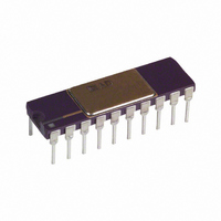
AD598AD Analog Devices Inc, AD598AD Datasheet - Page 8

AD598AD
Manufacturer Part Number
AD598AD
Description
IC LVDT SIGNAL COND 20-CDIP
Manufacturer
Analog Devices Inc
Type
Signal Conditionerr
Specifications of AD598AD
Rohs Status
RoHS non-compliant
Input Type
Voltage
Output Type
Voltage
Interface
LVDT
Current - Supply
15mA
Mounting Type
Through Hole
Package / Case
20-CDIP (0.300", 7.62mm)
Bandwidth
20kHz
Supply Voltage Min
13V
Supply Voltage Max
36V
Digital Ic Case Style
DIP
No. Of Pins
20
Operating Temperature Range
-40°C To +85°C
Temperature Coefficient
250ppm/°C
Application
Proving ring-weigh scale, synchronous opeation of multiple LVDTS
Converter Type
voltage to Frequency
Current, Output
6 mA (Min.)
Impedance, Input
200 Kiloohms (Typ.)
Package Type
Ceramic DIP
Temperature, Operating, Maximum
85 °C
Temperature, Operating, Minimum
-40 °C
Voltage, Operating
36 V (Max.)
Lead Free Status / RoHS Status
Contains lead / RoHS non-compliant
Available stocks
Company
Part Number
Manufacturer
Quantity
Price
Part Number:
AD598AD
Manufacturer:
ADI/亚德诺
Quantity:
20 000
AD598
13. Load current through R
14. C5 is a bypass capacitor in the range of 0.1 F to 1 F.
Gain Phase Characteristics
To use an LVDT in a closed loop mechanical servo application,
it is necessary to know the dynamic characteristics of the trans-
ducer and interface elements. The transducer itself is very quick
to respond once the core is moved. The dynamics arise prima-
rily from the interface electronics. Figures 13, 14 and 15 show
the frequency response of the AD598 LVDT Signal Condi-
tioner. Note that Figures 14 and 15 are basically the same; the
difference is frequency range covered. Figure 14 shows a wider
range of mechanical input frequencies at the expense of accu-
racy. Figure 15 shows a more limited frequency range with en-
hanced accuracy. The figures are transfer functions with the
input to be considered as a sinusoidally varying mechanical posi-
tion and the output as the voltage from the AD598; the units of
the transfer function are volts per inch. The value of C2, C3 and
C4, from Figure 7, are all equal and designated as a parameter
in the figures. The response is approximately that of two real
poles. However, there is appreciable excess phase at higher fre-
quencies. An additional pole of filtering can be introduced with
a shunt capacitor across R2, (see Figure 7); this will also in-
crease phase lag.
When selecting values of C2, C3 and C4 to set the bandwidth of
the system, a trade-off is involved. There is ripple on the “dc”
position output voltage, and the magnitude is determined by the
filter capacitors. Generally, smaller capacitors will give higher
system bandwidth and larger ripple. Figures 16 and 17 show the
magnitude of ripple as a function of C2, C3 and C4, again all
V
ps
SCHAEVITZ E100
+
R6, and flows back to V
tions, make sure the voltage drop across R5 is met as
defined in Step 12.
As a final check on the power supply voltages, verify that the
peak values of V
voltages at +V
6.8 F
30V
LVDT
Figure 12. Interconnection Diagram for Single
Supply Operation
0.1 F
15nF
C5
V
V
A
B
C2
C1
R1
S
and –V
A
R5
R6
and V
10
1
2
3
4
5
6
7
8
9
LEV 2
EXC 1
EXC 2
LEV 1
FREQ 1
FREQ 2
B1 FILT
B2 FILT
V
S
–V
B
L
.
PS
B
S
returns to the junction of R5 and
are at least 2.5 volts less than the
. Under maximum load condi-
AD598
FEEDBACK
OFFSET 2
OFFSET 1
OUT FILT
SIG OUT
SIG REF
A1 FILT
A2 FILT
+V
V
A
S
19
18
16
14
13
12
20
17
15
11
R4
R3
R2
33k
C4
C3
SIGNAL
REFERENCE
V
OUT
R
L
–8–
equal in value. Note also a shunt capacitor across R2 shown as a
parameter (see Figure 7). The value of R2 used was 81 k with
a Schaevitz E100 LVDT.
Figure 13. Gain and Phase Characteristics vs. Frequency
(0 kHz–10 kHz)
Figure 14. Gain and Phase Characteristics vs. Frequency
(0 kHz–50 kHz)
REV. A


