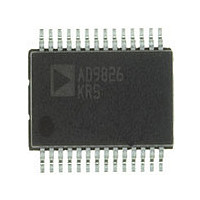
AD9826KRS Analog Devices Inc, AD9826KRS Datasheet - Page 18

AD9826KRS
Manufacturer Part Number
AD9826KRS
Description
IC IMAGE SGNL PROC 16BIT 28-SSOP
Manufacturer
Analog Devices Inc
Type
Image Sensorr
Datasheet
1.AD9826KRSZRL.pdf
(20 pages)
Specifications of AD9826KRS
Rohs Status
RoHS non-compliant
Input Type
Logic
Output Type
Logic
Interface
3-Wire Serial
Current - Supply
75mA
Mounting Type
Surface Mount
Package / Case
28-SSOP
Analog Front End Type
CCD
Analog Front End Category
Video
Interface Type
Serial (3-Wire)
Sample Rate
30MSPS
Input Voltage Range
2V
Operating Supply Voltage (min)
3/4.75V
Operating Supply Voltage (typ)
5V
Operating Supply Voltage (max)
5.25V
Resolution
16b
Supply Current
5/75mA
Number Of Adc's
1
Power Supply Type
Analog/Digital
Operating Temp Range
-40C to 85C
Operating Temperature Classification
Industrial
Mounting
Surface Mount
Pin Count
28
Package Type
SSOP
Number Of Channels
3
Lead Free Status / RoHS Status
Not Compliant
Available stocks
Company
Part Number
Manufacturer
Quantity
Price
Part Number:
AD9826KRS
Manufacturer:
ADI/亚德诺
Quantity:
20 000
Company:
Part Number:
AD9826KRSRL
Manufacturer:
MAXIM
Quantity:
94 126
Part Number:
AD9826KRSRL
Manufacturer:
ADI/亚德诺
Quantity:
20 000
Company:
Part Number:
AD9826KRSZ
Manufacturer:
AD
Quantity:
5 510
Part Number:
AD9826KRSZ
Manufacturer:
ADI/亚德诺
Quantity:
20 000
Part Number:
AD9826KRSZ-REEL
Manufacturer:
ADI/亚德诺
Quantity:
20 000
Part Number:
AD9826KRSZRL
Manufacturer:
ADI/亚德诺
Quantity:
20 000
Programmable Gain Amplifiers
The AD9826 uses one Programmable Gain Amplifier (PGA) for
each channel. Each PGA has a gain range from 1 (0 dB) to
6.0 (15.56 dB), adjustable in 64 steps. Figure 17 shows the
PGA gain as a function of the PGA register code. Although the
gain curve is approximately “linear in dB,” the gain in V/V var-
ies nonlinearly with register code, following the equation:
where G is the decimal value of the gain register contents, and
varies from 0 to 63.
AD9826
16
12
8
4
0
0
12
PGA REGISTER VALUE – Decimal
Gain
24
GAIN – dB
INPUTS
INPUTS
CLOCK
0.1 F
1 5 0
DATA
5V/3V
.
36
6 0
.
63
63
–
GAIN – V/V
G
CDSCLK2
CDSCLK1
(MSB) D7
48
ADCCLK
(LSB)D0
DRVDD
DRVSS
OEB
D6
D5
D4
D3
D2
D1
10
11
12
13
14
60
1
2
3
4
5
6
7
8
9
(Not to Scale)
63
TOP VIEW
AD9826
6.00
4.75
3.50
2.25
1.00
28
27
26
25
24
23
22
21
20
19
18
17
16
15
AVDD
AVSS
VINR
VING
CML
CAPT
CAPB
AVSS
AVDD
SLOAD
SCLK
SDATA
OFFSET
VINB
APPLICATIONS INFORMATION
Circuit and Layout Recommendations
The recommended circuit configuration for 3-Channel CDS
Mode operation is shown in Figure 18. The recommended
input coupling capacitor value is 0.1 F (see Circuit Operation
section for more details). A single ground plane is recommended
for the AD9826. A separate power supply may be used for
DRVDD, the digital driver supply, but this supply pin should
still be decoupled to the same ground plane as the rest of the
AD9826. The loading of the digital outputs should be mini-
mized, either by using short traces to the digital ASIC, or by
using external digital buffers. To minimize the effect of digital
transients during major output code transitions, the falling edge
of CDSCLK2 should occur coincident with or before the
rising edge of ADCCLK (see Figures 1 through 6 for timing).
All 0.1 F decoupling capacitors should be located as close as
possible to the AD9826 pins. When operating in 1CH or 2CH
Mode, the unused analog inputs should be grounded.
For 3-Channel SHA Mode, all of the above considerations also
apply, except that the analog input signals are directly connected
to the AD9826 without the use of coupling capacitors. The analog
input signals must already be dc-biased between 0 V and 4 V.
Also, the OFFSET pin should be grounded if the inputs to the
AD9826 are to be referenced to ground, or a dc offset voltage
should be applied to the OFFSET pin in the case where a coarse
offset needs to be removed from the inputs. (See Figure 16 and
the Circuit Operation section for more details.)
5V
0.1 F
0.1 F
0.1 F
5V
0.1 F
SERIAL
INTERFACE
10 F
0.1 F
0.1 F
0.1 F
0.1 F
0.1 F
0.1 F
1.0 F
RED INPUT
GREEN INPUT
BLUE INPUT


