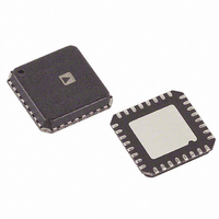
AD9943KCP Analog Devices Inc, AD9943KCP Datasheet - Page 6

AD9943KCP
Manufacturer Part Number
AD9943KCP
Description
IC CCD SIGNAL PROCESSOR 32-LFCSP
Manufacturer
Analog Devices Inc
Type
CCD Signal Processor, 10-Bitr
Datasheet
1.AD9943KCPZRL.pdf
(20 pages)
Specifications of AD9943KCP
Rohs Status
RoHS non-compliant
Input Type
Logic
Output Type
Logic
Interface
3-Wire Serial
Mounting Type
Surface Mount
Package / Case
32-LFCSP
Analog Front End Type
CCD
Analog Front End Category
Video
Interface Type
Serial (3-Wire)
Input Voltage Range
0.5V
Operating Supply Voltage (min)
2.7V
Operating Supply Voltage (typ)
3V
Operating Supply Voltage (max)
3.6V
Resolution
10b
Number Of Adc's
1
Power Supply Type
Analog/Digital
Operating Temp Range
-20C to 85C
Operating Temperature Classification
Commercial
Mounting
Surface Mount
Pin Count
32
Package Type
LFCSP EP
Number Of Channels
1
Current - Supply
-
Lead Free Status / RoHS Status
Not Compliant
Available stocks
Company
Part Number
Manufacturer
Quantity
Price
Company:
Part Number:
AD9943KCP
Manufacturer:
MOLEX
Quantity:
110
Company:
Part Number:
AD9943KCP
Manufacturer:
ADI
Quantity:
624
Company:
Part Number:
AD9943KCPZ
Manufacturer:
ADI
Quantity:
585
Part Number:
AD9943KCPZ
Manufacturer:
ADI/亚德诺
Quantity:
20 000
Company:
Part Number:
AD9943KCPZRL
Manufacturer:
SANYO
Quantity:
410
Company:
Part Number:
AD9943KCPZRL
Manufacturer:
ADI
Quantity:
15 000
AD9943/AD9944
TIMING SPECIFICATIONS
C
Table 5.
Parameter
SAMPLE CLOCKS
DATA OUTPUTS
SERIAL INTERFACE
1
Minimum CLPOB pulse width is for functional operation only. Wider typical pulses are recommended to achieve low noise clamp performance.
L
DATACLK, SHP, SHD Clock Period
DATACLK High/Low Pulse Width
SHP Pulse Width
SHD Pulse Width
CLPOB Pulse Width
SHP Rising Edge to SHD Falling Edge
SHP Rising Edge to SHD Rising Edge
Internal Clock Delay
Output Delay
Pipeline Delay
Maximum SCK Frequency
SL to SCK Setup Time
SCK to SL Hold Time
SDATA Valid to SCK Rising Edge Setup
SCK Falling Edge to SDATA Valid Hold
= 20 pF, f
SAMP
= 25 MHz. See CCD-mode timing in Figure 14 and Figure 15, and serial timing in Figure 10 and Figure 11.
1
Rev. B | Page 6 of 20
Symbol
t
t
t
t
t
t
t
t
t
f
t
t
t
t
CONV
ADC
SHP
SHD
COB
S1
S2
ID
OD
SCLK
LS
LH
DS
DH
Min
40
16
2
16
10
10
10
10
10
Typ
20
10
10
20
10
20
3.0
9.5
9
Max
Unit
ns
ns
ns
ns
Pixels
ns
ns
ns
ns
Cycles
MHz
ns
ns
ns
ns


