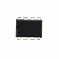
604-00038 Parallax Inc, 604-00038 Datasheet - Page 7

604-00038
Manufacturer Part Number
604-00038
Description
IC SENSOR TOUCH/PROXMTY 1CH 8DIP
Manufacturer
Parallax Inc
Series
QProx™r
Type
Capacitiver
Datasheet
1.604-00038.pdf
(12 pages)
Specifications of 604-00038
Touch Panel Interface
1, 2-Wire
Number Of Inputs/keys
1 Key
Resolution (bits)
14 b
Data Interface
Serial
Voltage Reference
Internal
Voltage - Supply
2.5 V ~ 5.5 V
Current - Supply
1.5mA
Operating Temperature
0°C ~ 70°C
Mounting Type
Through Hole
Package / Case
8-DIP (0.300", 7.62mm)
Output Type
Logic
Input Type
Logic
Product
Microcontroller Accessories
Lead Free Status / RoHS Status
Lead free / RoHS Compliant
Interface
-
Lead Free Status / RoHS Status
Lead free / RoHS Compliant, Lead free / RoHS Compliant
Figure 3-1 ESD Suppression Circuit
digital spikes, sags, and surges which can adversely affect
the QT113. The QT113 will track slow changes in Vdd, but it
can be affected by rapid voltage steps.
if desired, the supply can be regulated using a conventional
low current regulator, for example CMOS regulators that have
low quiescent currents.
3.5 ESD PROTECTION
In cases where the electrode is placed behind a dielectric
panel, the QT113 will usually be adequately protected from
direct static discharge. However, even with a plastic or glass
panel, transients can still flow into the electrode via induction,
or in extreme cases, via dielectric breakdown. Porous
materials may allow a spark to tunnel right through the
material; partially conducting materials like 'pink poly' will
conduct the ESD right to the electrode. Testing is required to
reveal any problems. The QT113 does have diode protection
on its terminals which can absorb and protect the device from
most induced discharges, up to 20mA; the usefulness of the
internal clamping will depending on the dielectric properties,
panel thickness, and rise time of the ESD transients.
ESD dissipation can be aided further with an added diode
protection network as shown in Figure 3-1, in extreme cases.
R
e3
2
3
4
OUT
O PT1
O PT2
+ 2 .5 to 5
1
8
V dd
V ss
S NS 2
G AIN
S NS 1
7
5
6
R
C
e2
s
R
e1
D
D
+
1
2
10µF
C 1
ELE C TRO DE
S E NS IN G
- 7 -
but Re1 should be low enough to permit at least 6
timeconstants of RC to occur during the charge and transfer
phases.
Re2 functions to isolate the transient from the QT113's Vdd
pin; values of around 1K ohms are reasonable.
As with all ESD protection networks, it is crucial that the
transients be led away from the circuit. PCB ground layout is
crucial; the ground connections to D1, D2, and C1 should all
go back to the power supply ground or preferably, if
available, a chassis ground connected to earth. The currents
should not be allowed to traverse the area directly under the
QT113.
If the QT113 is connected to an external circuit via a cable or
long twisted pair, it is possible for ground-bounce to cause
damage to the Out pin; even though the transients are led
away from the QT113 itself, the connected signal or power
ground line will act as an inductor, causing a high differential
voltage to build up on the Out wire with respect to ground. If
this is a possibility, the Out pin should have a resistance Re3
in series with it to limit current; this resistor should be as
large as can be tolerated by the load.
Because the charge and transfer times of the QT113
are relatively long, the circuit can tolerate very large
values of Re, even to 100k ohms in most cases where
electrode Cx is small. The added diodes shown
(1N4150 or equivalent low-C diodes, or a single BAV99
dual-diode) will shunt the ESD transients away from the
part, and Re1 will current limit the rest into the QT113's
own internal clamp diodes. C1 should be around 10µF
if it is to absorb positive transients from a human body
model standpoint without rising in value by more than 1
volt. If desired C1 can be replaced with an appropriate
Zener diode. Directly placing semiconductor transient
protection devices, Zeners, or MOV's on the sense lead
is not advised; these devices have extremely large
amounts of unstable parasitic C which will swamp the
QT113 and render it useless.
Re1 should be as large as possible given the load
value of Cx and the diode capacitances of D1 and D2,


