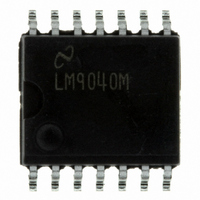
LM9040M/NOPB National Semiconductor, LM9040M/NOPB Datasheet - Page 6

LM9040M/NOPB
Manufacturer Part Number
LM9040M/NOPB
Description
IC SENSOR DUAL INTER AMP 14-SOIC
Manufacturer
National Semiconductor
Type
Sensor Interfacer
Datasheet
1.LM9040MNOPB.pdf
(12 pages)
Specifications of LM9040M/NOPB
Input Type
Differential
Output Type
Voltage
Current - Supply
8mA
Mounting Type
Surface Mount
Package / Case
14-SOIC (7.5mm Width)
Lead Free Status / RoHS Status
Lead free / RoHS Compliant
Interface
-
Other names
*LM9040M
*LM9040M/NOPB
LM9040M
*LM9040M/NOPB
LM9040M
www.national.com
In effect, the result is the same as forcing a bias current
through the Differential Input Impedance.
The bias current is defined as:
The Differential Input Impedance is defined as:
This bias voltage will be developed across the Differential In-
put Impedance (Z
the non-inverting input pin for I
a current path to ground. See
ating conditions I
Differential Input Filtering
Since each input is sampled independently, an anti-aliasing
filter is required at the amplifier inputs to ensure that the input
signal does not exceed the Nyquist frequency.
This external low-pass filter is implemented by adding a ca-
pacitor (C
forms an RC network across the differential inputs in con-
junction with the required external 4 kΩ resistors and the
differential input impedance (Z
should be small enough to have minimal effect on gain accu-
racy in the application, yet large enough to filter out unwanted
noise. Given that the F
the use of a 0.01 μF capacitor will generally provide adequate
filtering, with less than −0.4 dB of input attenuation at 500 Hz
and approximately −28 dB at 50 kHz. A larger value capacitor
can be used if needed, but a value larger than typically 0.02
μF will begin to dominate the cut-off frequency of the appli-
cation. This capacitor must be a low leakage and low ESR
type so that circuit performance is not degraded.
FIGURE 5. Equivalent Input Bias Circuit
DIFF
) across the differential input. See
BIAS
DIFF
will have a negligible effect on accuracy.
) if there is no other path available from
C
of the LM9040 is typically 500 Hz,
BIAS
Figure
DIFF
, and the inverting input has
). The capacitor selected
12372 Version 3 Revision 2
5. During normal oper-
Figure
1237215
6. This
Print Date/Time: 2009/12/02 10:13:43
6
Common Mode Filtering
The differential input sampling of the LM9040 actually re-
duces the effects of common mode input noise at low fre-
quencies. The time interval between the sampling of the
inverting input and the non-inverting input is one half of a clock
period. A change in the common mode voltage during this
short time interval can cause an error in the charge stored on
C
a sine-wave common mode voltage the minimum common
mode rejection is:
Where F
F
For a common mode sine wave signal having a frequency 100
Hz, and with a F
mode rejection would be:
If the common mode sine wave has a peak to peak value of
2V, the maximum voltage error at the output would be:
As this formula shows, the value of V
the frequency of the CMR signal. If the frequency is doubled,
the value of V
bypass capacitor (C
will help counter this problem. See
of this bypass capacitor creates a new problem in that the
differential input is no longer balanced. While the Lambda
sensor is cold (i.e. R
ence in CMR performance. As the Lambda sensor heats to
the operating temperature and the sensor resistance de-
creases, the common mode signal is no longer applied to both
inputs equally. This imbalance causes V
as R
full common mode signal, while the non-inverting input will
see an attenuated common mode signal.
The selection of the value of the CMR bypass capacitor needs
to be balanced with the need for reasonable reduction, or
elimination, of common mode signals with both cold and hot
sensors. Since normal operation will need to include consid-
eration of the entire impedance range of the sensor, a trade
off in overall application performance may be needed.
Generally, the value of the CMR bypass capacitor should be
kept as low as possible, and should not be larger than the
differential input filter capacitor. Values in the range of
0.001 μF to 0.01 μF will usually provide reasonable CMR re-
sults, but optimum results will need to be determined empiri-
cally, as the source of common mode signals will be unique
to each application.
CLOCK
IN
FIGURE 6. Differential and Common Mode Filtering
. This will result in an error seen on the output voltage. For
SENSOR
is the clock frequency.
CMR
CMRR = 2 •
CMRR = 2 • 3.14159 • 100 • 5E-6 • 4.53
decreases, as the non-inverting input will see the
is the frequency of the common mode signal, and
OUT(CM)
V
OUT(CM)
CLOCK
CMRR = 0.014 = −37 dB
CM
SENSOR
is also doubled. The addition of a small
π
) from the non-inverting input to ground
= 2V • 0.014 = 28 mV
• F
of 100 kHz, the minimum common
CMR
> 10 MegΩ) there is little differ-
• (0.5/F
Figure
OUT(CM)
CLOCK
6. However, the use
OUT(CM)
is proportional to
) • 4.53
to increase
1237216


