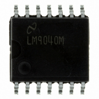
LM9040M/NOPB National Semiconductor, LM9040M/NOPB Datasheet - Page 8

LM9040M/NOPB
Manufacturer Part Number
LM9040M/NOPB
Description
IC SENSOR DUAL INTER AMP 14-SOIC
Manufacturer
National Semiconductor
Type
Sensor Interfacer
Datasheet
1.LM9040MNOPB.pdf
(12 pages)
Specifications of LM9040M/NOPB
Input Type
Differential
Output Type
Voltage
Current - Supply
8mA
Mounting Type
Surface Mount
Package / Case
14-SOIC (7.5mm Width)
Lead Free Status / RoHS Status
Lead free / RoHS Compliant
Interface
-
Other names
*LM9040M
*LM9040M/NOPB
LM9040M
*LM9040M/NOPB
LM9040M
www.national.com
dependent on the gain stage, and any signal on the non-in-
verting input will have no effect on the output. Each amplifier
has a comparator to monitor the voltage on the inverting input
pin. When the voltage on an inverting pin goes above typically
2.5V, the comparator will switch the output from the amplifier
output to the voltage divider stage. To fully implement this
function requires external pull-up resistors for each of the in-
In the cases where both the inverting and non-inverting pins
are open, the non-inverting condition (i.e.: voltage divider
across the output) will be the dominant condition.
Any common mode signal seen by inverting input pin should
not be allowed to exceed the Common Mode voltage range.
Exceeding the positive Common Mode voltage limit could
cause the inverting input pin voltage comparator to act as if
the inverting input pin is open. Since the comparator circuit is
not part of the switched capacitor network there is no fre-
quency limitation on the signal to the comparator. Any tran-
sient on the inverting input pin which goes above the
comparator threshold will immediately cause the output to
switch to the open sensor mode. The output will return to nor-
mal operation when the voltage on the inverting input falls
below the comparator threshold.
12372 Version 3 Revision 2
FIGURE 10. V
OUT
with Open Inverting Input
Print Date/Time: 2009/12/02 10:13:43
8
verting inputs. To minimize signal errors due to DC currents
through the 4 kΩ resistors, the pull-up resistors need to be
added in the application circuit between the 4 kΩ input resistor
and the connection to the Lambda sensor ground point. A
typical pull-up value of 51 kΩ to V
this condition, the effective resistance of the output stage will
be 3.5 kΩ typically. See
Supply Bypassing
For best performance the LM9040 requires a V
which is stable and noise free. The same 5V V
for the A/D converter is the recommended V
operation the device will generate current spikes coincident
with the clock edges. Inadequate bypassing will cause ex-
cessive clock noise on the outputs, as well as noise on the
V
minimum 0.1 μF capacitor to the Signal Ground pin, and
should be located as close to the device as possible. Some
applications may require an additional 4.7 μF tantalum ca-
pacitor, especially if there are several other switched capac-
itor devices running off the same 5V supply line. The Signal
and Digital Ground pins should be tied together as close to
the device as possible.
CC
line. The LM9030 V
Figure
CC
pin should be bypassed with a
10.
1237220
CC
is recommended. During
CC
REF
supply. During
supply used
CC
supply


