DS92LV1260TUJB/NOPB National Semiconductor, DS92LV1260TUJB/NOPB Datasheet - Page 3
DS92LV1260TUJB/NOPB
Manufacturer Part Number
DS92LV1260TUJB/NOPB
Description
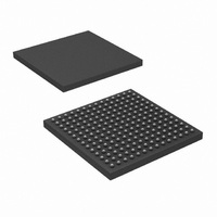
IC DESRL 6CH 10BIT BLVDS 196LBGA
Manufacturer
National Semiconductor
Datasheet
1.DS92LV1260TUJBNOPB.pdf
(17 pages)
Specifications of DS92LV1260TUJB/NOPB
Function
Deserializer
Data Rate
480Mbps
Input Type
LVDS
Output Type
LVTTL
Number Of Inputs
10
Number Of Outputs
1
Voltage - Supply
3 V ~ 3.6 V
Operating Temperature
-40°C ~ 85°C
Mounting Type
Surface Mount
Package / Case
196-LBGA
Lead Free Status / RoHS Status
Lead free / RoHS Compliant
Other names
*DS92LV1260TUJB
*DS92LV1260TUJB/NOPB
DS92LV1260TUJB
*DS92LV1260TUJB/NOPB
DS92LV1260TUJB
Available stocks
Company
Part Number
Manufacturer
Quantity
Price
Company:

Part Number:
DS92LV1260TUJB/NOPB
Manufacturer:
Texas Instruments
Quantity:
10 000


Over recommended operating supply and termperature ranges unless otherwise specified.(Note 2)
t
Deserializer Switching Characteristics
t
t
t
t
t
t
t
t
t
t
t
t
t
t
t
RFTT
RCP
RDC
CHTST
CLH
CHL
ROS
ROH
HZR
LZR
ZHR
ZLR
DD
DSR1
DSR2
RNM
Symbol
Electrical Characteristics
Basic functionality and specifications per deserializer channel will be similar to National Semiconductor’s DS92LV1212A.
Note 1: “Absolute Maximum Ratings” are those values beyond which the safety of the device cannot be guaranteed. They are not meant to imply that the devices
should be operated at these limits. The table of “Electrical Characteristics” specifies conditions of device operation.
Note 2: Typical values are given for Vcc = 3.3V and TA =25˚C
Note 3: Current into the device pins is defined as positive. Current out of device pins is defined as negative. Voltage are referenced to ground except VTH and VTL
which are differential voltages.
Note 4: Only one output should be shorted at a time. Do not exceed maximum package power dissipation capacity.
Note 5: For the purpose of specifying deserializer PLL performance t
the incoming data stream (SYNCPATs). t
is the time required to indicate lock for the powered-up and enabled deserializer when the input (RI+ and RI−) conditions change from not receiving data to receiving
synchronization patterns (SYNCPATs). The time to lock to random data is dependent upon the incoming data.
Note 6: t
Margin is Guaranteed By Design (GBD) using statistical analysis.
Note 7: Because the Bus LVDS serial data stream is not decoded, the maximum frequency of the CHTST output driver could be exceeded if the data stream were
switched to CHTST. The maximum frequency of the BUS LVDS input should not exceed the parallel clock rate.
RNM
REFCLK Transition Time
RCLK Period
RCLK Duty Cycle
Period of Bus LVDS signal
when CHTST is selected by
MUX
CMOS/TTL Low-to-High
Transition Time
CMOS/TTL High-to-Low
Transition Time
Rout Data Valid before
RCLK
Rout Data Valid after RCLK
High to TRI-STATE Delay
Low to TRI-STATE Delay
TRI-STATE to High Delay
TRI-STATE to Low Delay
Deserializer Delay
Deserializer PLL LOCK Time
from PWRDN (with
SYNCPAT)
Deserializer PLL Lock Time
from SYNCPAT
Deserializer Noise Margin
is a measure of how much phase noise (jitter)the deserializer can tolerate in the incoming data stream before bit errors occur. The Deserializer Noise
Parameter
DSR1
is the time required for the deserializer to indicate lock upon power-up or when leaving the power-down mode. t
Room Temp
Conditions
(Continued)
(Note 7)
Figure 2
Figure 2
Figure 1
Figure 3
(Note 5)
Figure 4
(Note 5)
(Note 6)
40MHz
3.3V
DSR1
and t
Pin/Freq.
CHTST
40MHz
20MHz
40MHz
20MHz
40MHz
20MHz
LOCK,
RCLK
RCLK
RCLK
DSR2
Rout,
3
are specified with the REFCLK running and stable, and specific conditions of
1.75*t
1.75*t
-0.4*t
0.4*t
1200
Min
450
25
43
25
RCP
RCP
RCP
RCP
+5
+6
1.75*t
1.75*t
1960
Typ
920
1.7
1.6
50
RCP
RCP
+7
+7
1.75*t
1.75*t
Max
62.5
55
10
10
12
12
10
RCP
8
6
6
3
2
5
RCP
www.national.com
+10
+9
Units
DSR2
ns
ns
ns
ns
ns
ns
ns
ns
ns
ns
ns
ns
ns
us
us
us
us
ps
ps
%
Related parts for DS92LV1260TUJB/NOPB
Image
Part Number
Description
Manufacturer
Datasheet
Request
R

Part Number:
Description:
National Semiconductor [8-Bit D/A Converter]
Manufacturer:
National Semiconductor
Datasheet:
Part Number:
Description:
National Semiconductor [Media Coprocessor]
Manufacturer:
National Semiconductor
Datasheet:
Part Number:
Description:
Digitally Controlled Tone and Volume Circuit with Stereo Audio Power Amplifier, Microphone Preamp Stage and National 3D Sound
Manufacturer:
National Semiconductor
Datasheet:
Part Number:
Description:
Digitally Controlled Tone and Volume Circuit with Stereo Audio Power Amplifier, Microphone Preamp Stage and National 3D Sound
Manufacturer:
National Semiconductor
Datasheet:
Part Number:
Description:
AC97 Rev 2 Codec with Sample Rate Conversion and National 3D Sound
Manufacturer:
National Semiconductor
Part Number:
Description:
Manufacturer:
National Semiconductor
Datasheet:
Part Number:
Description:
Manufacturer:
National Semiconductor
Datasheet:
Part Number:
Description:
General Purpose, Low Voltage, Low Power, Rail-to-Rail Output Operational Amplifiers
Manufacturer:
National Semiconductor
Datasheet:
Part Number:
Description:
8-bit 20 MSPS flash A/D converter.
Manufacturer:
National Semiconductor
Datasheet:
Part Number:
Description:
Low Noise Quad Operational Amplifier
Manufacturer:
National Semiconductor
Datasheet:
Part Number:
Description:
Quad Differential Line Receivers
Manufacturer:
National Semiconductor
Datasheet:
Part Number:
Description:
Quad High Speed Trapezoidal? Bus Transceiver
Manufacturer:
National Semiconductor
Datasheet:
Part Number:
Description:
Dual Line Receiver
Manufacturer:
National Semiconductor
Datasheet:
Part Number:
Description:
TTL to 10k ECL Level Translator with Latch
Manufacturer:
National Semiconductor
Datasheet: