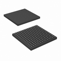
DS92LV1260TUJB/NOPB National Semiconductor, DS92LV1260TUJB/NOPB Datasheet - Page 8

DS92LV1260TUJB/NOPB
Manufacturer Part Number
DS92LV1260TUJB/NOPB
Description
IC DESRL 6CH 10BIT BLVDS 196LBGA
Manufacturer
National Semiconductor
Datasheet
1.DS92LV1260TUJBNOPB.pdf
(17 pages)
Specifications of DS92LV1260TUJB/NOPB
Function
Deserializer
Data Rate
480Mbps
Input Type
LVDS
Output Type
LVTTL
Number Of Inputs
10
Number Of Outputs
1
Voltage - Supply
3 V ~ 3.6 V
Operating Temperature
-40°C ~ 85°C
Mounting Type
Surface Mount
Package / Case
196-LBGA
Lead Free Status / RoHS Status
Lead free / RoHS Compliant
Other names
*DS92LV1260TUJB
*DS92LV1260TUJB/NOPB
DS92LV1260TUJB
*DS92LV1260TUJB/NOPB
DS92LV1260TUJB
Available stocks
Company
Part Number
Manufacturer
Quantity
Price
Company:
Part Number:
DS92LV1260TUJB/NOPB
Manufacturer:
Texas Instruments
Quantity:
10 000
www.national.com
Control Pins Truth Table
Note 8: The routing of the Din inputs to the Deserializers and to the CHTST outputs are dependent on the states of SEL [0:2].
Note 9: LOCK Active indicates that the LOCK output will reflect the state of it’s respective Deserializer with regard to the selected data stream.
Note 10: RCLK Active indicates that the RCLK will be running if the Deserializer is locked. The timing of RCLK [0:5] with respect to Rout [0:5][0:9] is determined
by RCLK_R/FFigure 5
Note 11: Rout n[0:9] and RCLK [0:5] are Tri-Stated when LOCKn[0:5] is High.
Functional Description
The DS92LV1260 combines six 1:10 deserializers into a
single chip. Each of the six deserializers accepts a BusLVDS
data stream from National Semiconductor’s DS92LV1021 or
DS92LV1023 Serializer. The deserializers then recover the
clock and data to deliver the resulting 10-bit wide words to
the outputs. A seventh serial data input provides n+1 redun-
dancy capability. The user can program the seventh input to
be an alternative input to any of the six deserializers. Which-
ever input is replaced by the seventh input is then routed to
the CHANNEL TEST (CHTST) pin on receiver output port.
Each of the 6 channels acts completely independent of each
other. Each independent channel has outputs for a 10-bit
wide data word, the recovered clock out, and the lock-detect
output.
The DS92LV1260 has three operating states: Initialization,
Data Transfer, and Resynchronization. In addition, there are
two passive states: Powerdown and TRI-STATE.
The following sections describe each operating mode and
passive state.
Initialization
Before the DS92LV1260 receives and deserializes data, it
and the transmitting serializer devices must initialize the link.
Initialization refers to synchronizing the Serializer’s and the
Deserializer’s PLL’s to local clocks. The local clocks must be
the same frequency or within a specified range if from differ-
ent sources. After all devices synchronize to local clocks, the
Deserializers synchronize to the Serializers as the second
and final initialization step.
Step 1: After applying power to the Deserializer, the outputs
are held in TRI-STATE and the on-chip power-sequencing
circuitry disables the internal circuits. When V
V
the local clock (REFCLK). A local on-board oscillator or other
source provides the specified clock input to the REFCLK pin.
Step 2: The Deserializer PLL must synchronize to the Seri-
alizer to complete the initialization. Refer to the Serializer
cc
H
H
H
H
H
H
L
OK (2.1V), the PLL in each deserializer begins locking to
H
H
H
H
H
X
L
H
H
H
H
X
X
L
H
H
H
X
X
L
L
H
H
H
L
L
X
X
(Continued)
cc
Rout 3 (0:9)(Note
Rout 4 (0:9)(Note
Rout 5 (0:9)(Note
Din6 Decoded to
Din6 Decoded to
Din6 Decoded to
reaches
Din6 is not
Din6 is not
Decoded
Decoded
11)
11)
11)
Z
Z
8
data sheet for the proper operation during this step of the
Initialization State. The Deserializer identifies the rising clock
edge in a synchronization pattern or random data and after
80 clock cycles will synchronize to the data stream from the
serializer. At the point where the Deserializer’s PLL locks to
the embedded clock, the LOCKn pin goes low and valid data
appears on the output. Note that this differs from pervious
deserializers where the LOCKn signal was not synchronous
to valid data appearing on the outputs.
Data Transfer
After initialization, the serializer transfers data to the deseri-
alizers. The serial data stream includes a start and stop bit
appended by the serializer, which frame the ten data bits.
The start bit is always high and the stop bit is always low.
The start and stop bits also function as clock bits embedded
in the serial stream.
The Serializer transmits the data and clock bits (10+2 bits) at
12 times the TCLK frequency. For example, if TCLK is 40
MHz, the serial rate is 40 X 12 = 480 Mbps. Since only 10
bits are from input data, the serial ’payload’ rate is 10 times
the TCLK frequency. For instance, if TCLK = 40 MHz, the
payload data is 40 X 10 = 400 Mbps. TCLK is provided by
the data source and must be in the range 20 MHz to 40 MHz
nominal.
When one of six Deserializer channels synchronizes to the
input from a Serializer, it drives its LOCKn pin low and
synchronously delivers valid data on the output. The Dese-
rializer locks to the embedded clock, uses it to generate
multiple internal data strobes, and drives the embedded
clock to the RCLKn pin. The RCLKn is synchronous to the
data on the ROUT[n0:n9] pins. While LOCKn is low, data on
ROUT [n0:n9] is valid. Otherwise, ROUT[n0:n9] is invalid.
All ROUT, LOCK, and RCLK signals will drive a minimum of
three CMOS input gates (15pF load) with a 40 MHz clock.
This amount of drive allows bussing outputs of two Deseri-
alizers and a destination ASIC. REN controls TRI-STATE
of all the outputs.
decoded)
decoded)
decoded)
decoded)
Din3 (not
Din4 (not
Din5 (not
Din6 (not
Z
Z
Z
Active(Note 9)
Active(Note 9)
Active(Note 9)
Active(Note 9)
Active(Note 9)
Active(Note 9)
Z
Active(Notes 10,
Active(Notes 10,
Active(Notes 10,
Active(Notes 10,
Active(Notes 10,
11)
11)
11)
11)
11)
Z
Z
™


