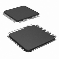
DS90CR484AVJDX/NOPB National Semiconductor, DS90CR484AVJDX/NOPB Datasheet - Page 5

DS90CR484AVJDX/NOPB
Manufacturer Part Number
DS90CR484AVJDX/NOPB
Description
IC DESERIALIZER 48BIT 100TQFP
Manufacturer
National Semiconductor
Datasheet
1.DS90CR483AVJDNOPB.pdf
(24 pages)
Specifications of DS90CR484AVJDX/NOPB
Function
Serializer/Deserializer
Data Rate
5.38Gbps
Input Type
LVDS
Output Type
CMOS, TTL
Number Of Inputs
8
Number Of Outputs
48
Voltage - Supply
3 V ~ 3.6 V
Operating Temperature
-10°C ~ 70°C
Mounting Type
Surface Mount
Package / Case
100-TQFP, 100-VQFP
Number Of Elements
8
Number Of Receivers
8
Number Of Drivers
48
Operating Supply Voltage (typ)
3.3V
Differential Input High Threshold Voltage
100mV
Diff. Input Low Threshold Volt
-100mV
Differential Output Voltage
450mV
Power Dissipation
2.3W
Operating Temp Range
-10C to 70C
Operating Temperature Classification
Commercial
Mounting
Surface Mount
Pin Count
100
Package Type
TQFP
Lead Free Status / RoHS Status
Lead free / RoHS Compliant
Other names
DS90CR484AVJDX
Available stocks
Company
Part Number
Manufacturer
Quantity
Price
Company:
Part Number:
DS90CR484AVJDX/NOPB
Manufacturer:
Texas Instruments
Quantity:
10 000
LLHT
LHLT
TBIT
TPPOS
TJCC
TCCS
TSTC
THTC
TPDL
TPLLS
TPDD
CLHT
CHLT
RCOP
RCOH
RCOL
RSRC
RHRC
RPDL
RPLLS
RPDD
Symbol
Symbol
Transmitter Switching Characteristics
Over recommended operating supply and temperature ranges unless otherwise specified.
Receiver Switching Characteristics
Over recommended operating supply and temperature ranges unless otherwise specified.
LVDS Low-to-High Transition Time, (Figure 2),
PRE = 0.75V (disabled)
LVDS Low-to-High Transition Time, (Figure 2),
PRE = Vcc (max)
LVDS High-to-Low Transition Time, (Figure 2),
PRE = 0.75V (disabled)
LVDS High-to-Low Transition Time, (Figure 2),
PRE = Vcc (max)
Transmitter Bit Width
Transmitter Pulse Positions - Normalized f = 33 to 70
Transmitter Jitter - Cycle-to-Cycle ((Note 8)
TxOUT Channel to Channel Skew
TxIN Setup to TxCLK IN, (Figure 5)
TxIN Hold to TxCLK IN, (Figure 5)
Transmitter Propagation Delay - Latency, (Figure 7)
Transmitter Phase Lock Loop Set, (Figure 9)
Transmitter Powerdown Delay, (Figure 11)
CMOS/TTL Low-to-High Transition Time, (Figure 3), Rx
data out
CMOS/TTL Low-to-High Transition Time, (Figure 3), Rx
clock out
CMOS/TTL High-to-Low Transition Time, (Figure 3), Rx
data out
CMOS/TTL High-to-Low Transition Time, (Figure 3), Rx
clock out
RxCLK OUT Period, (Figure 6)
RxCLK OUT High Time, (Figure 6),
(Note 4)
RxCLK OUT Low Time, (Figure 6),
(Note 4)
RxOUT Setup to RxCLK OUT, (Figure
6), (Note 4)
RxOUT Hold to RxCLK OUT, (Figure
6), (Note 4)
Receiver Propagation Delay - Latency, (Figure 8)
Receiver Phase Lock Loop Set, (Figure 10)
Receiver Powerdown Delay, (Figure 12)
Parameter
Parameter
f = 112 MHz
f = 66 MHz
f = 112 MHz
f = 66 MHz
f = 112 MHz
f = 66 MHz
f = 112 MHz
f = 66 MHz
MHz
f = 70 to 112
MHz
5
1.5(TCIP)+3.72
3(TCIP)+4.0
−250
−200
8.928
Min
2.5
Min
3.5
6.0
3.5
6.0
2.4
3.6
3.4
7.0
0
1.5(TCIP)+4.4
3(TCIP)+4.8
1/7 TCIP
0.14
0.11
0.16
0.11
Typ
Typ
50
40
0
0
T
1.5(TCIP)+6.24
3(TCIP)+6.5
+250
+200
Max
100
100
Max
30.3
0.7
0.6
0.8
0.7
10
2.0
1.0
2.0
1.0
10
1
www.national.com
Units
Units
ms
ms
ns
ns
ns
ns
ns
ps
ps
ps
ps
ns
ns
ns
ns
ns
ns
ns
ns
ns
ns
ns
ns
ns
ns
ns
ns
ns
ns
µs


