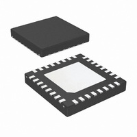
DS90LV804TSQX/NOPB National Semiconductor, DS90LV804TSQX/NOPB Datasheet - Page 6

DS90LV804TSQX/NOPB
Manufacturer Part Number
DS90LV804TSQX/NOPB
Description
IC BUFFER/REPEATR LVDS 4CH 32LLP
Manufacturer
National Semiconductor
Type
Bufferr
Datasheet
1.DS90LV804TSQXNOPB.pdf
(10 pages)
Specifications of DS90LV804TSQX/NOPB
Tx/rx Type
LVDS
Delay Time
3.2ns
Capacitance - Input
3.5pF
Voltage - Supply
3.15 V ~ 3.45 V
Current - Supply
140mA
Mounting Type
Surface Mount
Package / Case
32-LLP
Lead Free Status / RoHS Status
Lead free / RoHS Compliant
Other names
DS90LV804TSQX
Available stocks
Company
Part Number
Manufacturer
Quantity
Price
Company:
Part Number:
DS90LV804TSQX/NOPB
Manufacturer:
TI/NSC
Quantity:
8 322
www.national.com
Feature Descriptions
INTERNAL TERMINATIONS
The DS90LV804 has integrated termination resistors on both
the input and outputs. The inputs have a 100Ω resistor across
the differential pair, placing the receiver termination as close
as possible to the input stage of the device. The LVDS outputs
also contain an integrated 100Ω ohm termination resistor, this
resistor is used to reduce the effects of Near End Crosstalk
(NEXT) and does not take the place of the 100 ohm termina-
tion at the inputs to the receiving device. The integrated
terminations improve signal integrity and decrease the exter-
nal component count resulting in space savings.
OUTPUT CHARACTERISTICS
The output characteristics of the DS90LV804 have been op-
timized for point-to-point backplane and cable applications,
and are not intended for multipoint or multidrop signaling.
TRI-STATE MODE
The EN input activates a hardware TRI-STATE mode. When
the TRI-STATE mode is active (EN=L), all input and output
6
buffers and internal bias circuitry are powered off and dis-
abled. Outputs are tri-stated in TRI-STATE mode. When ex-
iting TRI-STATE mode, there is a delay associated with
turning on bandgap references and input/output buffer circuits
as indicated in the LVDS Output Switching Characteristics
INPUT FAILSAFE BIASING
External pull up and pull down resistors may be used to pro-
vide enough of an offset to enable an input failsafe under
open-circuit conditions. This configuration ties the positive
LVDS input pin to V
LVDS input pin is tied to GND by a pull down resistor. The pull
up and pull down resistors should be in the 5kΩ to 15kΩ range
to minimize loading and waveform distortion to the driver. The
common-mode bias point ideally should be set to approxi-
mately 1.2V (less than 1.75V) to be compatible with the
internal circuitry. Please refer to application note AN-1194
“Failsafe Biasing of LVDS Interfaces” for more information.
DD
thru a pull up resistor and the negative


