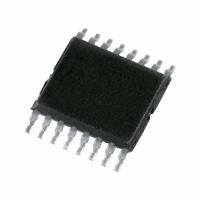
PCA9546APW,112 NXP Semiconductors, PCA9546APW,112 Datasheet - Page 6

PCA9546APW,112
Manufacturer Part Number
PCA9546APW,112
Description
IC I2C SWITCH 4CH 16TSSOP
Manufacturer
NXP Semiconductors
Datasheet
1.PCA9546ABS118.pdf
(25 pages)
Specifications of PCA9546APW,112
Package / Case
16-TSSOP
Applications
4-Channel I²C Switcher
Interface
I²C, SMBus
Voltage - Supply
2.3 V ~ 5.5 V
Mounting Type
Surface Mount
Product
Multiplexer
Number Of Lines (input / Output)
4.0 / 1.0
Propagation Delay Time
0.3 ns
Supply Voltage (max)
3.6 V
Supply Voltage (min)
2.3 V
Maximum Operating Temperature
+ 85 C
Minimum Operating Temperature
- 40 C
Mounting Style
SMD/SMT
Number Of Input Lines
4.0
Number Of Output Lines
1.0
Power Dissipation
400 mW
Lead Free Status / RoHS Status
Lead free / RoHS Compliant
Lead Free Status / RoHS Status
Lead free / RoHS Compliant, Lead free / RoHS Compliant
Other names
568-5026
935275813112
PCA9546APW
PCA9546APW,112
PCA9546APW
935275813112
PCA9546APW
PCA9546APW,112
PCA9546APW
NXP Semiconductors
PCA9546A_5
Product data sheet
6.2.1 Control register definition
6.2 Control register
Following the successful acknowledgement of the slave address, the bus master will send
a byte to the PCA9546A, which will be stored in the control register. If multiple bytes are
received by the PCA9546A, it will save the last byte received. This register can be written
and read via the I
One or several SCx/SDx downstream pair, or channel, is selected by the contents of the
control register. This register is written after the PCA9546A has been addressed. The
4 LSBs of the control byte are used to determine which channel is to be selected. When a
channel is selected, the channel will become active after a STOP condition has been
placed on the I
the channel is made active, so that no false conditions are generated at the time of
connection.
Table 4.
Remark: Several channels can be enabled at the same time. Example: B3 = 0, B2 = 1,
B1 = 1, B0 = 0, means that channel 0 and channel 3 are disabled and channel 1 and
channel 2 are enabled. Care should be taken not to exceed the maximum bus
capacitance.
D7
X
X
X
X
0
Fig 6.
D6
X
X
X
X
0
Control register
Control register: Write—channel selection; Read—channel status
2
D5
X
X
X
X
0
C-bus. This ensures that all SCx/SDx lines will be in a HIGH state when
2
C-bus.
D4
X
X
X
X
0
Rev. 05 — 2 July 2009
X
7
X
6
B3
X
X
X
0
1
0
5
X
X
4
B2
X
X
0
1
X
0
channel selection bits
B3
3
(read/write)
B2
2
B1
X
0
1
X
X
0
B1
1
4-channel I
B0
0
B0
0
1
X
X
X
0
002aab190
channel 0
channel 1
channel 2
channel 3
Command
channel 0 disabled
channel 0 enabled
channel 1 disabled
channel 1 enabled
channel 2 disabled
channel 2 enabled
channel 3 disabled
channel 3 enabled
no channel selected;
power-up/reset default state
2
C-bus switch with reset
PCA9546A
© NXP B.V. 2009. All rights reserved.
6 of 25


