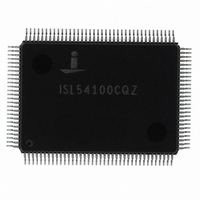
ISL54100CQZ Intersil, ISL54100CQZ Datasheet - Page 17

ISL54100CQZ
Manufacturer Part Number
ISL54100CQZ
Description
IC REGENERATOR TMDS 4:1 128-MQFP
Manufacturer
Intersil
Datasheet
1.ISL54102CQZ.pdf
(21 pages)
Specifications of ISL54100CQZ
Applications
Multimedia Displays, Test Equipment
Interface
I²C
Voltage - Supply
3 V ~ 3.6 V
Package / Case
128-MQFP, 128-PQFP
Mounting Type
Surface Mount
Rohs Compliant
Yes
Lead Free Status / RoHS Status
Lead free / RoHS Compliant
Available stocks
Company
Part Number
Manufacturer
Quantity
Price
Company:
Part Number:
ISL54100CQZ
Manufacturer:
Intersil
Quantity:
128
Part Number:
ISL54100CQZ
Manufacturer:
INTERSIL
Quantity:
20 000
• Avoid vias for all 3 high speed TMDS pairs. Vias add
• For each TMDS channel, the trace lengths of the 3 TMDS
• The trace length of the clock pair is not critical at all.
• Minimize capacitance on all TMDS lines. The lower the
• Maintain a constant, solid ground (or power) plane under
planes and 100Ω with respect to each other. Failure to
meet this requirement will increase reflections, shrinking
the available eye.
inductance which causes a discontinuity in the
characteristic impedance of the trace. Keep all the traces
on the top (or the bottom) of the PCB. The TMDS clock
can have vias if necessary, since it is lower speed and less
critical. If you must use a via, ensure the vias are
symmetrical (put identical vias in both lines of the
differential pair).
pairs (0, 1 and 2) should ideally be the same to reduce
inter channel skew introduced by the board.
Since the clock is only used as a frequency reference, its
phase/delay is inconsequential. In addition, since the
TMDS clock frequency is 1/10th the pixel rate, the clock
signal itself is much more noise-immune. So liberties
(such as vias and circuitous paths) can be taken when
routing the clock lines.
capacitance, the sharper the rise and fall times.
the 3 high speed TMDS signals. Do not route the signals
over gaps in the ground plane or over other traces.
FIGURE 12. SUB-OPTIMAL BYPASS CAPACITOR LAYOUT
V
+
EQUIVALENT CIRCUIT
C
BYPASS
VIAS
GND
GROUND PLANE
TO
POWER PLANE
C
R
BYPASS
TRACE
17
POWER
PLANE
VIA TO
R
R
VIA
TRACE
GND
V
+
GND
IC
V
+
IC
ISL54100, ISL54101, ISL54102
• Ideally each supply should be bypassed to ground with a
0.1µF capacitor. Minimize trace length and vias to
minimize inductance and maximize noise rejection.
Figure 12 demonstrates a common but non-ideal PCB
layout and its equivalent circuit. The additional trace
resistance between the bypass capacitor and the power
supply/IC reduces its effectiveness. Figure 13
demonstrates a better layout. In this case there is still
series trace resistance (it is impossible to completely
eliminate it), but now it is being put to good use, as part of
a “T” filter, attenuating supply noise before it gets to the IC,
and reducing the amount of IC-generated noise that gets
injected into the supply. Follow the good supply bypassing
rules shown in Figure 13 to the extent possible.
FIGURE 13. OPTIMAL (“T”) BYPASS CAPACITOR LAYOUT
V
+
EQUIVALENT CIRCUIT
R
POWER
VIA TO
PLANE
VIA
C
R
BYPASS
TRACE
POWER PLANE
GROUND PLANE
C
VIAS
GND
TO
BYPASS
R
TRACE
GND
V
+
GND
IC
V
+
IC
June 4, 2008
FN6275.5


