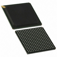
PI7C9X20505GPBNDE Pericom Semiconductor, PI7C9X20505GPBNDE Datasheet - Page 29

PI7C9X20505GPBNDE
Manufacturer Part Number
PI7C9X20505GPBNDE
Description
IC PCIE PACKET SWITCH 256BGA
Manufacturer
Pericom Semiconductor
Series
GreenPacket™r
Specifications of PI7C9X20505GPBNDE
Applications
Data Transport
Interface
Advanced Configuration Power Interface (ACPI)
Package / Case
256-PBGA
Mounting Type
Surface Mount
Lead Free Status / RoHS Status
Lead free / RoHS Compliant
Voltage - Supply
-
Available stocks
Company
Part Number
Manufacturer
Quantity
Price
Company:
Part Number:
PI7C9X20505GPBNDE
Manufacturer:
Pericom
Quantity:
180
June 2009 – Revision 1.5
Pericom Semiconductor
ADDRESS
26h
28h
32h
34h
36h
38h
42h
44h
46h
48h
50h
52h
E0h (Port 3)
E0h: Bit [24]
F0h (Port 3)
F0h: Bit [28]
80h (Port 3)
80h: Bit[21]
144h (Port 3)
144h: Bit [4]
ECh (Port 3)
ECh: Bit [26:24]
154h (Port 3)
154h: Bit [7:1]
E0h (Port 4)
E0h: Bit [24]
F0h (Port 4)
F0h: Bit [28]
80h (Port 4)
80h: Bit[21]
144h (Port 4)
144h: Bit [4]
ECh (Port 4)
ECh: Bit [26:24]
154h (Port 4)
154h: Bit [7:1]
F4h (Port 1)
F4h: Bit [15:0]
F4h (Port 2)
F4h: Bit [15:0]
F4h (Port 3)
F4h: Bit [15:0]
F4h (Port 4)
F4h: Bit [15:0]
F4h (Port 1)
F4h: Bit [31:16]
F4h (Port 2)
F4h: Bit [31:16]
F4h (Port 3)
F4h: Bit [31:16]
F4h (Port 4)
F4h: Bit [31:16]
15Ch (Port 0)
15Ch: Bit [22:16]
160h: Bit [7:0]
15Ch (Port 1)
15Ch: Bit [22:16]
160h: Bit [7:0]
PCI CFG
OFFSET
DESCRIPTION
PCIe Capability Slot Implemented for Port 3
Slot Clock Configuration for Port 3
Device specific Initialization for Port 3
LPVC Count for Port 3
Port Number for Port 3
VC0 TC/VC Map for Port 3
PCIe Capability Slot Implemented for Port 4
Slot Clock Configuration for Port 4
Device specific Initialization for Port 4
LPVC Count for Port 4
Port Number for Port 4
VC0 TC/VC Map for Port 4
Slot Capability 0 of Port 1
Slot Capability 0 of Port 2
Slot Capability 0 of Port 3
Slot Capability 0 of Port 4
Slot Capability 1 of Port 1
Slot Capability 1 of Port 2
Slot Capability 1 of Port 3
Slot Capability 1 of Port 4
VC1 MAX Time Slot and TC/VC Map for Port 0
VC1 MAX Time Slot and TC/VC Map for Port 1
Page 29 of 81
Bit [0]: When set, the slot is implemented for Port 3
Bit [1]: When set, the component uses the clock provided on the
Bit [2]: When set, the DSI is required
Bit [3]: When set, the VC1 is allocated to LPVC of Egress Port 3
Bit [6:4]: It represents the logic port numbering for physical port
3
Bit [15:9]: When set, it indicates the corresponding TC is
mapped into VC0
Bit [0]: When set, the slot is implemented for Port 4
Bit [1]: When set, the component uses the clock provided on the
Bit [2]: When set, the DSI is required
Bit [3]: When set, the VC1 is allocated to LPVC of Egress Port 4
Bit [6:4]: It represents the logic port numbering for physical port
4
Bit [15:9]: When set, it indicates the corresponding TC is
mapped into VC0
Bit [15:0]: Mapping to the low word of slot capability register
Bit [15:0]: Mapping to the low word of slot capability register
Bit [15:0]: Mapping to the low word of slot capability register
Bit [15:0]: Mapping to the low word of slot capability register
Bit [15:0]: Mapping to the high word of slot capability register
Bit [15:0]: Mapping to the high word of slot capability register
Bit [15:0]: Mapping to the high word of slot capability register
Bit [15:0]: Mapping to the high word of slot capability register
Bit [6:0]: The maximum time slot supported by VC1
Bit [15:8]: When set, it indicates the corresponding TC is
mapped into VC1
Bit [6:0]: The maximum time slot supported by VC1
Bit [15:8]: When set, it indicates the corresponding TC is
mapped into VC1
Connector
Connector
5Port-5Lane PCI Express Switch
GreenPacket
PI7C9X20505GP
Datasheet
TM
Family


