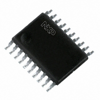
PCA9518PW,118 NXP Semiconductors, PCA9518PW,118 Datasheet - Page 11

PCA9518PW,118
Manufacturer Part Number
PCA9518PW,118
Description
IC I2C BUS HUB 5-CH 20TSSOP
Manufacturer
NXP Semiconductors
Datasheet
1.PCA9518D118.pdf
(21 pages)
Specifications of PCA9518PW,118
Package / Case
20-TSSOP
Applications
Buffer
Interface
I²C
Voltage - Supply
3 V ~ 3.6 V
Mounting Type
Surface Mount
Logic Family
PCA9518
Operating Supply Voltage
3 V to 3.6 V
Power Dissipation
300 mW
Operating Temperature Range
- 40 C to + 85 C
Input Voltage
5 V
Logic Type
I2C Bus
Maximum Clock Frequency
400 KHz
Mounting Style
SMD/SMT
Output Voltage
5 V
Lead Free Status / RoHS Status
Lead free / RoHS Compliant
Lead Free Status / RoHS Status
Lead free / RoHS Compliant, Lead free / RoHS Compliant
Other names
935272403118
PCA9518PW-T
PCA9518PW-T
PCA9518PW-T
PCA9518PW-T
NXP Semiconductors
10. Dynamic characteristics
Table 5.
[1]
[2]
[3]
PCA9518_5
Product data sheet
Symbol
t
t
t
t
t
t
t
t
t
PHL
PLH
PHL1
PLH1
PLH2
THL
TLH
su
h
The SDA and SCL propagation delays are dominated by rise times or fall times. The fall times are mostly internally controlled and are
only sensitive to load capacitance. The rise times are RC time constant controlled and therefore a specific numerical value can only be
given for fixed RC time constants.
The SDA HIGH to LOW propagation delay includes the fall time from V
SCL fall time from the quiescent HIGH (usually V
included which make the fall time almost independent of load capacitance.
The SDA or SCL LOW to HIGH propagation delay includes the rise time constant from the quiescent LOW to 0.5V
or EXPSCL2, the rise time constant for the quiescent LOW to 0.5V
the quiescent external driven LOW to 0.7V
external resistance and total capacitance for the various nodes.
Parameter
HIGH to LOW propagation delay
LOW to HIGH propagation delay
HIGH to LOW propagation delay 1
LOW to HIGH propagation delay 1
LOW to HIGH propagation delay 2
HIGH to LOW output transition time
LOW to HIGH output transition time
set-up time
hold time
Dynamic characteristics
Fig 7.
AC waveforms
EXPSDA1 or EXPSCL1
EXPSDA2 or EXPSCL2
CC
output SDA or SCL
input SDA or SCL
for the SDA or SCL output. All of these rise times are RC time constants determined by the
CC
Rev. 05 — 2 December 2008
) to below 0.3V
Conditions
SDA to SDAn, or
SCL to SCLn;
SDA to SDAn, or
SCL to SCLn;
EXPSDA1 to SDA, or
EXPSCL1 to SCL;
EXPSDA1 to SDA, or
EXPSCL1 to SCL;
EXPSDA2 to SDA, or
EXPSCL2 to SCL;
SDA, SCL;
SDA, SCL;
enable to START condition
enable after STOP condition
0.7V
t
PHL1
t
PHL2
Figure 7
Figure 7
CC
CC
CC
0.5V
. The SDA and SCL outputs have edge rate control circuits
t
t
Figure 7
Figure 7
for the EXPSDA1 or EXPSCL1, and the rise time constant from
PHL
PHL1
0.7V
CC
CC
0.52 V
to 0.5V
CC
Figure 7
Figure 7
Figure 7
0.3V
t
THL
0.4 V
0.5V
CC
CC
CC
t
THL
of the EXPSDA1 or EXPSCL1 pins and the SDA or
0.3V
effective
stretch
CC
Expandable 5-channel I
[1][2]
[1][3]
0.4 V
t
PLH2
0.5V
0.3V
0.5V
Min
105
110
109
130
160
58
-
300
300
CC
0.3V
CC
CC
t
CC
TLH
t
TLH
Typ
202
259
193
153
234
110
0.85 RC
-
-
0.7V
t
t
PCA9518
002aae328
PLH1
PLH2
0.7V
© NXP B.V. 2008. All rights reserved.
CC
t
CC
PLH
CC
for the EXPSDA1
Max
389
265
327
179
279
187
-
-
-
2
C-bus hub
11 of 21
Unit
ns
ns
ns
ns
ns
ns
ns
ns
ns


