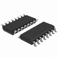
UJA1023T/2R04/C,51 NXP Semiconductors, UJA1023T/2R04/C,51 Datasheet - Page 17

UJA1023T/2R04/C,51
Manufacturer Part Number
UJA1023T/2R04/C,51
Description
IC CAN/LIN I/O SLAVE 16-SOIC
Manufacturer
NXP Semiconductors
Datasheet
1.UJA1023T2R04C51.pdf
(49 pages)
Specifications of UJA1023T/2R04/C,51
Applications
LIN Controller
Interface
SPI
Voltage - Supply
6.5 V ~ 27 V
Package / Case
16-SOIC (3.9mm Width)
Mounting Type
Surface Mount
Lead Free Status / RoHS Status
Lead free / RoHS Compliant
Other names
935285403518
Available stocks
Company
Part Number
Manufacturer
Quantity
Price
Part Number:
UJA1023T/2R04/C,51
Manufacturer:
NXP/恩智浦
Quantity:
20 000
NXP Semiconductors
UJA1023
Product data sheet
Table 16.
Byte
D0
D1
D2
D3
D4
D5
D6 and D7 7 to 0
First I/O configuration data block bit description
Bit
7 to 0
7 to 0
7 to 0
7 and 6
5 and 4
3
2 to 0
7 to 0
7 to 0
All information provided in this document is subject to legal disclaimers.
NAD[7:0]
-
ADCIN[2:0]
LSE[7:0]
OM0_[7:0],
Symbol
PCI[7:0]
SID[7:0]
IM[1:0]
RxDL
HSE[7:0]
OM1_[7:0]
Rev. 5 — 17 August 2010
Description
Slave node address (NAD). NAD values are in the range from
1 to 127, while 0 and 128 to 255 are reserved for other
purposes. The slave node address is assigned with the
assign NAD command (see
Protocol control information.
Service identifier. As SlaveResp the RSID value will be 0xF4.
00 for first configuration data block.
Pin INH mode. Mode will be changed after PxReq or PxResp
Receive data length. Message PxReq contains two data
bytes if RxDL = 0 and three data bytes if RxDL = 1.
Analog source channel selection. The number of ADCIN[2:0]
determines which of the P7 to P0 input is used. For example
if ADCIN[2:0] = 101 then P5 will be the input. ADCIN[2:0] is
used only if ADC mode is selected (IM[1:0] = 01) and
RxDL = 0 (No analog input selection at PxReq).
High-side enable for I/O pin Px.
Low-side enable for I/O pin Px.
Output mode for I/O pin Px.
OM1_x
0
0
1
1
00 = external regulator (control of external voltage
regulator)
01 = ADC
10 = reserved, if selected both bits will be logic 1
11 = switch open
OM0_x
0
1
0
1
level
reserved
cyclic sense
PWM
Table
5).
UJA1023
© NXP B.V. 2010. All rights reserved.
LIN-I/O slave
17 of 49


