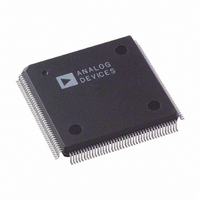
AD9887KS-140 Analog Devices Inc, AD9887KS-140 Datasheet - Page 29

AD9887KS-140
Manufacturer Part Number
AD9887KS-140
Description
IC INTRFACE ANALOG/DVI 160-MQFP
Manufacturer
Analog Devices Inc
Datasheet
1.AD9887AKSZ-100.pdf
(40 pages)
Specifications of AD9887KS-140
Rohs Status
RoHS non-compliant
Applications
Graphic Cards, VGA Interfaces
Interface
Analog and Digital
Voltage - Supply
3.15 V ~ 3.45 V
Package / Case
160-MQFP, 160-PQFP
Mounting Type
Surface Mount
Available stocks
Company
Part Number
Manufacturer
Quantity
Price
Company:
Part Number:
AD9887KS-140
Manufacturer:
ADI
Quantity:
440
Part Number:
AD9887KS-140
Manufacturer:
ADI/亚德诺
Quantity:
20 000
2-WIRE SERIAL CONTROL REGISTER DETAIL
CHIP IDENTIFICATION
00
PLL DIVIDER CONTROL
01
02
CLOCK GENERATOR CONTROL
03
03
7–0 Chip Revision
Bits 7 through 4 represent functional revisions to the
analog interface. Changes in these bits will generally
indicate that software and/or hardware changes will be
required for the chip to work properly. Bits 3 through 0
represent nonfunctional related revisions and are reset to
0000 whenever the MSBs are changed. Changes in these
bits are considered transparent to the user.
7–0 PLL Divide Ratio MSBs
The eight most significant bits of the 12-bit PLL divide ratio
PLLDIV. (The operational divide ratio is PLLDIV + 1.)
The PLL derives a pixel clock from the incoming Hsync
signal. The pixel clock frequency is then divided by an
integer value, such that the output is phase-locked to
Hsync. This PLLDIV value determines the number of
pixel times (pixels plus horizontal blanking overhead) per
line. This is typically 20% to 30% more than the number
of active pixels in the display.
The 12-bit value of the PLL divider supports divide ratios
from 221 to 4095. The higher the value loaded in this
register, the higher the resulting clock frequency with
respect to a fixed Hsync frequency.
VESA has established some standard timing specifications,
which will assist in determining the value for PLLDIV as
a function of horizontal and vertical display resolution
and frame rate (Table VII).
However, many computer systems do not conform pre-
cisely to the recommendations, and these numbers should
be used only as a guide. The display system manufacturer
should provide automatic or manual means for optimizing
PLLDIV. An incorrectly set PLLDIV will usually produce
one or more vertical noise bars on the display. The greater
the error, the greater the number of bars produced.
The power-up default value of PLLDIV is 1693
(PLLDIVM = 69h, PLLDIVL = Dxh).
The AD9887 updates the full divide ratio only when the
LSBs are changed. Writing to this register by itself will not
trigger an update.
7–4 PLL Divide Ratio LSBs
The four least significant bits of the 12-bit PLL divide ratio
PLLDIV. The operational divide ratio is PLLDIV + 1.
The power-up default value of PLLDIV is 1693
(PLLDIVM = 69h, PLLDIVL = Dxh).
The AD9887 updates the full divide ratio only when this
register is written.
7 TEST
6–5 VCO Range Select
Two bits that establish the operating range of the clock
generator.
VCORNGE must be set to correspond with the desired
operating frequency (incoming pixel rate).
Set to One
03
04
CLAMP TIMING
05
The PLL gives the best jitter performance at high fre-
quencies. For this reason, in order to output low pixel
rates and still get good jitter performance, the PLL actu-
ally operates at a higher frequency but then divides down
the clock rate afterwards. Table X shows the pixel rates
for each VCO range setting. The PLL output divisor is
automatically selected with the VCO range setting.
VCORNGE
00
01
10
11
The power-up default value is = 01.
4–2 CURRENT Charge Pump Current
Three bits that establish the current driving the loop filter
in the clock generator.
CURRENT
000
001
010
011
100
101
110
111
See Table VII for the recommended CURRENT settings.
The power-up default value is CURRENT = 001.
7–3 Clock Phase Adjust
A five-bit value that adjusts the sampling phase in 32 steps
across one pixel time. Each step represents an 11.25° shift
in sampling phase.
The power-up default value is 16.
7–0 Clamp Placement
An eight-bit register that sets the position of the internally
generated clamp.
When EXTCLMP = 0, a clamp signal is generated inter-
nally, at a position established by the clamp placement and
for a duration set by the clamp duration. Clamping is
started (Clamp Placement) pixel periods after the trailing
edge of Hsync. The clamp placement may be programmed
to any value between 1 and 255. A value of 0 is not
supported.
The clamp should be placed during a time that the input
signal presents a stable black-level reference, usually the
back porch period between Hsync and the image.
When EXTCLMP = 1, this register is ignored.
Table XI. Charge Pump Currents
Table X. VCO Ranges
Pixel Rate Range
12–35
35–70
70–110
110–140
Current ( A)
50
100
150
250
350
500
750
1500
AD9887


