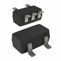
NX3V1G66GW,125 NXP Semiconductors, NX3V1G66GW,125 Datasheet - Page 5

NX3V1G66GW,125
Manufacturer Part Number
NX3V1G66GW,125
Description
IC SWITCH SPST 5TSSOP
Manufacturer
NXP Semiconductors
Datasheet
1.NX3V1G66GW125.pdf
(18 pages)
Specifications of NX3V1G66GW,125
Package / Case
6-TSSOP (5 lead), SC-88A, SOT-353
Function
Switch
Circuit
1 x SPST- NO
On-state Resistance
250 mOhm
Voltage Supply Source
Single Supply
Voltage - Supply, Single/dual (±)
1.4 V ~ 4.3 V
Current - Supply
150nA
Operating Temperature
-40°C ~ 125°C
Mounting Type
Surface Mount
Switch Configuration
SPST
On Resistance (max)
0.8 Ohm (Typ) @ 1.4 V
On Time (max)
42 ns @ 1.6 V
Off Time (max)
22 ns @ 1.6 V
Supply Voltage (max)
4.3 V
Supply Voltage (min)
1.4 V
Maximum Power Dissipation
250 mW
Maximum Operating Temperature
+ 125 C
Mounting Style
SMD/SMT
Minimum Operating Temperature
- 40 C
Lead Free Status / RoHS Status
Lead free / RoHS Compliant
Lead Free Status / RoHS Status
Lead free / RoHS Compliant, Lead free / RoHS Compliant
Other names
568-4760-2
935286667125
NX3V1G66GW,125
NX3V1G66GW-G
NX3V1G66GW-G
935286667125
NX3V1G66GW,125
NX3V1G66GW-G
NX3V1G66GW-G
Available stocks
Company
Part Number
Manufacturer
Quantity
Price
Company:
Part Number:
NX3V1G66GW,125
Manufacturer:
TI
Quantity:
1 448
NXP Semiconductors
Table 7.
At recommended operating conditions; voltages are referenced to GND (ground 0 V).
Table 8.
At recommended operating conditions; voltages are referenced to GND (ground = 0 V); for graphs see
NX3V1G66
Product data sheet
Symbol Parameter
C
C
C
Symbol
R
Fig 5.
I
S(OFF)
S(ON)
ON(peak)
input
capacitance
OFF-state
capacitance
ON-state
capacitance
V
Test circuit for measuring OFF-state leakage
current
V
Parameter
ON resistance
(peak)
I
Static characteristics
Resistance R
IL
= 0.3 V or V
V I
11.1 Test circuits
11.2 ON resistance
nE
nZ
CC
0.3 V; V
ON
Conditions
V
CC
Conditions
V
I
GND
SW
I
V
V
V
V
V
= GND to V
CC
CC
CC
CC
CC
= 100 mA; see
O
…continued
= V
nY
= 1.4 V
= 1.65 V
= 2.3 V
= 2.7 V
= 4.3 V
CC
I
S
0.3 V or 0.3 V.
All information provided in this document is subject to legal disclaimers.
001aag488
CC
;
V O
Rev. 6 — 21 December 2010
Figure 7
Min
Fig 6.
Low-ohmic single-pole single-throw analog switch
T
-
-
-
amb
Min
T
-
-
-
-
-
amb
= 40 C to +85 C T
Typ
205
1.0
V
Test circuit for measuring ON-state leakage
current
70
= 25 C
I
Typ
0.25
0.25
= 0.3 V or V
0.8
0.5
0.3
V
IH
[1]
Max
V I
I
-
-
-
S
Max
0.45
0.45
1.9
0.8
0.5
CC
nE
nZ
0.3 V; V
T
Min
amb
amb
-
-
-
V
CC
Min
= 40 C to +125 C
GND
= 40 C to +125 C Unit
-
-
-
-
-
O
= open circuit.
NX3V1G66
(85 C)
Max
nY
Figure 8
-
-
-
001aag489
© NXP B.V. 2010. All rights reserved.
V O
(125 C)
Max
2.1
0.9
0.6
0.5
0.5
Max
to
-
-
-
Figure
5 of 18
Unit
pF
pF
pF
14.


