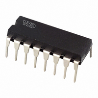
HEF4052BP,652 NXP Semiconductors, HEF4052BP,652 Datasheet - Page 3

HEF4052BP,652
Manufacturer Part Number
HEF4052BP,652
Description
IC MUX/DEMUX DUAL 4X1 16DIP
Manufacturer
NXP Semiconductors
Series
4000Br
Type
Analog Multiplexerr
Specifications of HEF4052BP,652
Package / Case
16-DIP (0.300", 7.62mm)
Function
Multiplexer/Demultiplexer
Circuit
2 x 4:1
On-state Resistance
175 Ohm
Voltage Supply Source
Single Supply
Voltage - Supply, Single/dual (±)
3 V ~ 15 V, -18 V ~ 0.5 V
Operating Temperature
-40°C ~ 85°C
Mounting Type
Through Hole
Number Of Channels
2 Channel
On Resistance (max)
2500 Ohm @ 5 V
On Time (max)
260 ns @ 5 V
Off Time (max)
205 ns @ 5 V
Supply Voltage (max)
15.5 V
Supply Voltage (min)
4.5 V
Mounting Style
Through Hole
Number Of Switches
Dual
Package
16PDIP
Maximum On Resistance
2500@5V Ohm
Maximum Propagation Delay Bus To Bus
305@5V|150@10V|100@15V ns
Maximum Low Level Output Current
10 mA
Multiplexer Architecture
4:1
Maximum Turn-off Time
205@5V ns
Maximum Turn-on Time
260@5V ns
Power Supply Type
Single
Lead Free Status / RoHS Status
Lead free / RoHS Compliant
Lead Free Status / RoHS Status
Lead free / RoHS Compliant, Lead free / RoHS Compliant
Other names
568-3109-5
933282430652
HEF4052BPN
933282430652
HEF4052BPN
Philips Semiconductors
FUNCTION TABLE
Notes
1. H = HIGH state (the more positive voltage)
RATINGS
Limiting values in accordance with the Absolute Maximum System (IEC 134)
Note
1. To avoid drawing V
January 1995
Supply voltage (with reference to V
Dual 4-channel analogue multiplexer/demultiplexer
E
H
L = LOW state (the less positive voltage)
X = state is immaterial
the bidirectional switch must not exceed 0,4 V. If the switch current flows into terminal Z, no V
of terminals Y, in this case there is no limit for the voltage drop across the switch, but the voltages at Y and Z may
not exceed V
L
L
L
L
INPUTS
A
H
H
X
L
L
1
DD
or V
A
H
H
X
L
L
0
DD
EE
current out of terminal Z, when switch current flows into terminals Y, the voltage drop across
.
Y
Y
Y
Y
0A
1A
2A
3A
CHANNEL
DD
Z
Z
Z
Z
none
A
A
A
A
ON
)
; Y
; Y
; Y
; Y
Fig.3 Schematic diagram (one switch).
0B
1B
2B
3B
Z
Z
Z
Z
B
B
B
B
3
V
EE
18 to
0,5 V
DD
Product specification
current will flow out
HEF4052B
MSI


