HEF4016BP,652 NXP Semiconductors, HEF4016BP,652 Datasheet - Page 2
HEF4016BP,652
Manufacturer Part Number
HEF4016BP,652
Description
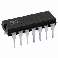
IC SWITCH QUAD 2X1 14DIP
Manufacturer
NXP Semiconductors
Series
4000Br
Specifications of HEF4016BP,652
Package / Case
14-DIP (0.300", 7.62mm)
Function
Switch
Circuit
4 x 2:1
On-state Resistance
350 Ohm
Current - Supply
4µA
Operating Temperature
-40°C ~ 85°C
Mounting Type
Through Hole
Switch Configuration
SPST
On Resistance (max)
8000 Ohm (Typ) @ 5 V
On Time (max)
80 ns @ 5 V
Off Time (max)
130 ns @ 5 V
Supply Voltage (max)
15.5 V
Supply Voltage (min)
4.5 V
Maximum Power Dissipation
400 mW
Maximum Operating Temperature
+ 85 C
Mounting Style
Through Hole
Minimum Operating Temperature
- 40 C
Lead Free Status / RoHS Status
Lead free / RoHS Compliant
Lead Free Status / RoHS Status
Lead free / RoHS Compliant, Lead free / RoHS Compliant
Other names
568-3079-5
933282410652
HEF4016BPN
933282410652
HEF4016BPN


Philips Semiconductors
DESCRIPTION
The HEF4016B has four independent analogue switches
(transmission gates). Each switch has two input/output
terminals (Y/Z) and an active HIGH enable input (E). When
E is connected to V
between Y and Z is established (ON condition). When E is
connected to V
PINNING
APPLICATION INFORMATION
Some examples of applications for the HEF4016B are:
January 1995
E
Y
Z
0
0
0
Signal gating
Modulation
Demodulation
Chopper
Fig.3 Schematic diagram
Quadruple bilateral switches
to E
to Y
to Z
3
3
3
(one switch).
enable inputs
input/output terminals
input/output terminals
SS
Fig.1 Functional diagram.
the switch is disabled and a high
DD
a low impedance bidirectional path
2
impedance between Y and Z is established (OFF
condition). Current through a switch will not cause
additional V
terminals of the switch is maintained within the supply
voltage range; V
electrically equivalent terminals.
HEF4016BP(N): 14-lead DIL; plastic (SOT27-1)
HEF4016BD(F): 14-lead DIL; ceramic (cerdip) (SOT73)
HEF4016BT(D): 14-lead SO; plastic (SOT108-1)
( ): Package Designator North America
DD
current provided the voltage at the
DD
Fig.2 Pinning diagram.
(V
Y
, V
Z
)
V
SS
Product specification
. Inputs Y and Z are
HEF4016B
gates
Related parts for HEF4016BP,652
Image
Part Number
Description
Manufacturer
Datasheet
Request
R

Part Number:
Description:
Hef4016b Quadruple Bilateral Switches
Manufacturer:
NXP Semiconductors
Datasheet:
Part Number:
Description:
NXP Semiconductors designed the LPC2420/2460 microcontroller around a 16-bit/32-bitARM7TDMI-S CPU core with real-time debug interfaces that include both JTAG andembedded trace
Manufacturer:
NXP Semiconductors
Datasheet:

Part Number:
Description:
NXP Semiconductors designed the LPC2458 microcontroller around a 16-bit/32-bitARM7TDMI-S CPU core with real-time debug interfaces that include both JTAG andembedded trace
Manufacturer:
NXP Semiconductors
Datasheet:
Part Number:
Description:
NXP Semiconductors designed the LPC2468 microcontroller around a 16-bit/32-bitARM7TDMI-S CPU core with real-time debug interfaces that include both JTAG andembedded trace
Manufacturer:
NXP Semiconductors
Datasheet:
Part Number:
Description:
NXP Semiconductors designed the LPC2470 microcontroller, powered by theARM7TDMI-S core, to be a highly integrated microcontroller for a wide range ofapplications that require advanced communications and high quality graphic displays
Manufacturer:
NXP Semiconductors
Datasheet:
Part Number:
Description:
NXP Semiconductors designed the LPC2478 microcontroller, powered by theARM7TDMI-S core, to be a highly integrated microcontroller for a wide range ofapplications that require advanced communications and high quality graphic displays
Manufacturer:
NXP Semiconductors
Datasheet:
Part Number:
Description:
The Philips Semiconductors XA (eXtended Architecture) family of 16-bit single-chip microcontrollers is powerful enough to easily handle the requirements of high performance embedded applications, yet inexpensive enough to compete in the market for hi
Manufacturer:
NXP Semiconductors
Datasheet:
Part Number:
Description:
The XA-S3 device is a member of Philips Semiconductors? XA(eXtended Architecture) family of high performance 16-bitsingle-chip microcontrollers
Manufacturer:
NXP Semiconductors
Datasheet:

Part Number:
Description:
The NXP BlueStreak LH75401/LH75411 family consists of two low-cost 16/32-bit System-on-Chip (SoC) devices
Manufacturer:
NXP Semiconductors
Datasheet:
Part Number:
Description:
The NXP LPC3130/3131 combine an 180 MHz ARM926EJ-S CPU core, high-speed USB2
Manufacturer:
NXP Semiconductors
Datasheet:
Part Number:
Description:
The NXP LPC3141 combine a 270 MHz ARM926EJ-S CPU core, High-speed USB 2
Manufacturer:
NXP Semiconductors
Part Number:
Description:
The NXP LPC3143 combine a 270 MHz ARM926EJ-S CPU core, High-speed USB 2
Manufacturer:
NXP Semiconductors

Part Number:
Description:
The NXP LPC3152 combines an 180 MHz ARM926EJ-S CPU core, High-speed USB 2
Manufacturer:
NXP Semiconductors
Part Number:
Description:
The NXP LPC3154 combines an 180 MHz ARM926EJ-S CPU core, High-speed USB 2
Manufacturer:
NXP Semiconductors