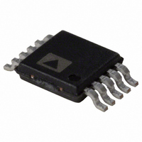
ADG621BRMZ Analog Devices Inc, ADG621BRMZ Datasheet - Page 5

ADG621BRMZ
Manufacturer Part Number
ADG621BRMZ
Description
IC SWITCH DUAL SPST 10MSOP
Manufacturer
Analog Devices Inc
Datasheet
1.ADG622BRMZ.pdf
(12 pages)
Specifications of ADG621BRMZ
Function
Switch
Circuit
2 x SPST - NO
On-state Resistance
5.5 Ohm
Voltage Supply Source
Dual Supply
Voltage - Supply, Single/dual (±)
±2.7 V ~ 5.5 V
Current - Supply
0.0001µA
Operating Temperature
-40°C ~ 85°C
Mounting Type
Surface Mount
Package / Case
10-TFSOP, 10-MSOP (0.118", 3.00mm Width)
Analog Switch Type
SPST
No. Of Channels
2
Bandwidth
230MHz
On State Resistance Max
4ohm
Turn Off Time
45ns
Turn On Time
75ns
Supply Voltage Range
± 2.7V To ± 5.5V
Lead Free Status / RoHS Status
Lead free / RoHS Compliant
Available stocks
Company
Part Number
Manufacturer
Quantity
Price
Part Number:
ADG621BRMZ
Manufacturer:
ADI/亚德诺
Quantity:
20 000
Company:
Part Number:
ADG621BRMZ-REEL
Manufacturer:
ANALOG
Quantity:
790
ABSOLUTE MAXIMUM RATINGS
T
Table 3.
Parameter
V
V
V
Analog Inputs
Digital Inputs
Peak Current, S or D
Continuous Current, S or D
Operating Temperature Range
Storage Temperature Range
Junction Temperature
MSOP Package
Lead Soldering
Pb-Free Soldering
1
Overvoltages at INx, S, or D must be clamped by internal diodes. Currents
should be limited to the maximum ratings given.
DD
DD
SS
A
Industrial (B Version)
θ
θ
Lead Temperature, Soldering
IR Reflow, Peak Temperature
Reflow, Peak Temperature
Time at Peak Temperature
= 25°C, unless otherwise noted.
to GND
to V
to GND
JA
JC
(10 sec)
Thermal Impedance
Thermal Impedance
SS
1
1
Rating
13 V
−0.3 V to +6.5 V
+0.3 V to –6.5 V
V
–0.3 V to V
whichever occurs first
100 mA (pulsed at 1 ms,
10% duty cycle maximum)
50 mA
–40°C to +85°C
–65°C to +150°C
150°C
206°C/W
44°C/W
300°C
220°C
260(+0/−5)°C
20 sec to 40 sec
SS
– 0.3 V to V
DD
+ 0.3 V or 30 mA,
DD
+ 0.3 V
Rev. B | Page 5 of 12
Stresses above those listed under Absolute Maximum Ratings
may cause permanent damage to the device. This is a stress
rating only; functional operation of the device at these or any
other conditions above those listed in the operational sections
of this specification is not implied. Exposure to absolute
maximum rating conditions for extended periods may affect
device reliability.
Only one absolute maximum rating may be applied at any
one time.
Table 4. ADG621/ADG622 Truth Table
ADG621 INx
0
1
Table 5. ADG623 Truth Table
IN1
0
0
1
1
ESD CAUTION
IN2
0
1
0
1
ADG622 INx
1
0
ADG621/ADG622/ADG623
Switch S1
Off
Off
On
On
Switch Sx Condition
Off
On
Switch S2
On
Off
On
Off


