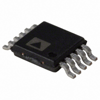
ADG621BRMZ Analog Devices Inc, ADG621BRMZ Datasheet - Page 7

ADG621BRMZ
Manufacturer Part Number
ADG621BRMZ
Description
IC SWITCH DUAL SPST 10MSOP
Manufacturer
Analog Devices Inc
Datasheet
1.ADG622BRMZ.pdf
(12 pages)
Specifications of ADG621BRMZ
Function
Switch
Circuit
2 x SPST - NO
On-state Resistance
5.5 Ohm
Voltage Supply Source
Dual Supply
Voltage - Supply, Single/dual (±)
±2.7 V ~ 5.5 V
Current - Supply
0.0001µA
Operating Temperature
-40°C ~ 85°C
Mounting Type
Surface Mount
Package / Case
10-TFSOP, 10-MSOP (0.118", 3.00mm Width)
Analog Switch Type
SPST
No. Of Channels
2
Bandwidth
230MHz
On State Resistance Max
4ohm
Turn Off Time
45ns
Turn On Time
75ns
Supply Voltage Range
± 2.7V To ± 5.5V
Lead Free Status / RoHS Status
Lead free / RoHS Compliant
Available stocks
Company
Part Number
Manufacturer
Quantity
Price
Part Number:
ADG621BRMZ
Manufacturer:
ADI/亚德诺
Quantity:
20 000
Company:
Part Number:
ADG621BRMZ-REEL
Manufacturer:
ANALOG
Quantity:
790
TERMINOLOGY
I
Positive supply current.
I
Negative supply current
V
Analog voltage on Terminal D and Terminal S.
R
Ohmic resistance between Terminal D and Terminal S.
R
On resistance flatness is defined as the difference between the
maximum and minimum value of on resistance as measured
over the specified analog signal range.
∆R
On resistance match between any two channels.
I
Source leakage current with the switch off.
I
Drain leakage current with the switch off.
I
Channel leakage current with the switch on.
V
Maximum input voltage for Logic 0.
V
Minimum input voltage for Logic 1.
I
Input current of the digital input.
C
Off switch source capacitance. Measured with reference to
ground.
C
Off switch drain capacitance. Measured with reference to
ground.
C
On switch capacitance. Measured with reference to ground.
DD
SS
S
D
D
INL
ON
FLAT (ON)
D
INL
INH
S
D
D
, I
(Off)
(Off)
, C
(Off)
ON
(V
(Off)
(I
S
(On)
INH
S
S
)
(On)
)
Rev. B | Page 7 of 12
C
Digital input capacitance.
t
Delay time between the 50% and the 90% points of the digital
input and switch on condition.
t
Delay time between the 50% and the 90% points of the digital
input and switch off condition.
t
On or off time measured between the 90% points of both
switches when switching from one address state to another.
Charge Injection
A measure of the glitch impulse transferred from the digital
input to the analog output during on-off switching.
Off Isolation
A measure of an unwanted signal coupling through an
off switch.
Crosstalk
A measure of an unwanted signal that is coupled through from
one channel to another as a result of parasitic capacitance.
−3 dB Bandwidth
The frequency at which the output is attenuated by 3 dB.
On Response
The frequency response of the on switch.
Insertion Loss
The attenuation between the input and output ports of the
switch when the switch is in the on condition and is due to
the on resistance of the switch.
ON
OFF
BBM
IN
ADG621/ADG622/ADG623


