ADG431BNZ Analog Devices Inc, ADG431BNZ Datasheet - Page 2
ADG431BNZ
Manufacturer Part Number
ADG431BNZ
Description
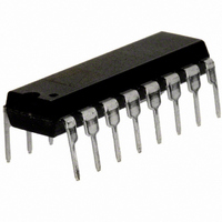
IC SWITCH QUAD SPST 16DIP
Manufacturer
Analog Devices Inc
Series
LC²MOSr
Datasheet
1.ADG433BRZ.pdf
(8 pages)
Specifications of ADG431BNZ
Function
Switch
Circuit
4 x SPST - NO
On-state Resistance
24 Ohm
Voltage Supply Source
Single Supply
Voltage - Supply, Single/dual (±)
5V, 12V
Current - Supply
0.1µA
Operating Temperature
-40°C ~ 85°C
Mounting Type
Through Hole
Package / Case
16-DIP (0.300", 7.62mm)
Analog Switch Type
SPST
No. Of Channels
4
On State Resistance Max
17ohm
Turn Off Time
60ns
Turn On Time
90ns
Supply Voltage Range
4.5V To 5.5V
Operating Temperature Range
-40°C To +85°C
Lead Free Status / RoHS Status
Lead free / RoHS Compliant
Available stocks
Company
Part Number
Manufacturer
Quantity
Price


ADG431/ADG432/ADG433–SPECIFICATIONS
Dual Supply
Parameter
ANALOG SWITCH
LEAKAGE CURRENTS
DIGITAL INPUTS
DYNAMIC CHARACTERISTICS
POWER REQUIREMENTS
NOTES
1
Specifications subject to change without notice.
Guaranteed by design, not subject to production test.
Analog Signal Range
R
R
R
R
Source OFF Leakage I
Drain OFF Leakage I
Channel ON Leakage I
Input High Voltage, V
Input Low Voltage, V
Input Current
C
t
t
Break-Before-Make Time Delay, t
(ADG433 Only)
Charge Injection
OFF Isolation
Channel-to-Channel Crosstalk
C
C
C
I
I
I
Power Dissipation
ON
OFF
DD
SS
L
ON
ON
ON
ON
IN
S
D
D
I
INL
, C
(OFF)
(OFF)
Digital Input Capacitance
vs. V
Drift
Match
S
or I
(ON)
D
INH
(V
S
)
(V
DD
= +15 V
D
INL
INH
S
D
(OFF)
(OFF)
, I
S
(ON)
10%, V
1
D
SS
= –15 V
+25 C
17
24
15
0.5
5
± 0.05
± 0.25
± 0.05
± 0.25
± 0.1
± 0.35
0.005
9
90
60
25
5
68
85
9
9
35
0.0001
0.1
0.0001
0.1
0.0001
0.1
B Version
10%, V
L
–40 C to
+85 C
V
26
± 2
± 2
± 3
2.4
0.8
± 0.02
165
130
0.2
0.2
0.2
7.7
= +5 V
DD
to V
SS
10%, GND = O V, unless otherwise noted.)
Unit
V
Ω typ
Ω max
% typ
%/°C typ
% typ
nA typ
nA max
nA typ
nA max
nA typ
nA max
V min
V max
µA typ
µA max
pF typ
ns typ
ns max
ns typ
ns max
ns typ
pC typ
dB typ
dB typ
pF typ
pF typ
pF typ
µA typ
µA max
µA typ
µA max
µA typ
µA max
µW max
1
Test Conditions/Comments
V
V
V
V
V
Test Circuit 2
V
Test Circuit 2
V
Test Circuit 3
V
V
R
V
R
V
R
V
Test Circuit 5
V
Test Circuit 6
R
Test Circuit 7
R
Test Circuit 8
f = 1 MHz
f = 1 MHz
f = 1 MHz
V
Digital Inputs = 0 V or 5 V
D
DD
D
DD
D
D
D
IN
DD
L
S
L
S
L
S1
S
L
L
DD
= ± 10 V; Test Circuit 4
= ± 10 V; Test Circuit 4
= 0 V, R
= 300 Ω, C
= 300 Ω, C
= 300 Ω, C
= 50 Ω, C
= 50 Ω, C
= ± 8.5 V, I
= 0 V, I
= ± 15.5 V, V
= ± 15.5 V, V
= V
= V
= V
= +13.5 V, V
= +16.5 V, V
= +15 V, V
= +16.5 V, V
S
S2
INL
= ± 15.5 V;
= +10 V;
S
or V
S
= –10 mA
= 0 Ω, C
L
L
L
L
L
S
= 5 pF, f = 1 MHz;
= 5 pF, f = 1 MHz;
INH
SS
= –10 mA;
= 35 pF;
= 35 pF;
= 35 pF;
S
S
SS
SS
SS
=
=
= –15 V
= –13.5 V
= –16.5 V
= –16.5 V
L
15.5 V;
15.5 V;
= 10 nF;
Related parts for ADG431BNZ
Image
Part Number
Description
Manufacturer
Datasheet
Request
R

Part Number:
Description:
±1.7g Dual-Axis IMEMS Accelerometer Evaluation Board
Manufacturer:
Analog Devices Inc
Datasheet:

Part Number:
Description:
Inertial Sensor Evaluation System
Manufacturer:
Analog Devices Inc
Datasheet:
Part Number:
Description:
Manufacturer:
Analog Devices Inc
Datasheet:
Part Number:
Description:
Manufacturer:
Analog Devices Inc
Datasheet:
Part Number:
Description:
Manufacturer:
Analog Devices Inc
Datasheet:
Part Number:
Description:
Manufacturer:
Analog Devices Inc
Datasheet:
Part Number:
Description:
Manufacturer:
Analog Devices Inc
Datasheet:
Part Number:
Description:
Manufacturer:
Analog Devices Inc
Datasheet:
Part Number:
Description:
Manufacturer:
Analog Devices Inc
Datasheet:
Part Number:
Description:
Manufacturer:
Analog Devices Inc
Datasheet:
Part Number:
Description:
Manufacturer:
Analog Devices Inc
Datasheet:
Part Number:
Description:
Manufacturer:
Analog Devices Inc
Datasheet:
Part Number:
Description:
Manufacturer:
Analog Devices Inc
Datasheet: