ADG431BNZ Analog Devices Inc, ADG431BNZ Datasheet - Page 4
ADG431BNZ
Manufacturer Part Number
ADG431BNZ
Description
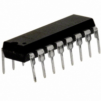
IC SWITCH QUAD SPST 16DIP
Manufacturer
Analog Devices Inc
Series
LC²MOSr
Datasheet
1.ADG433BRZ.pdf
(8 pages)
Specifications of ADG431BNZ
Function
Switch
Circuit
4 x SPST - NO
On-state Resistance
24 Ohm
Voltage Supply Source
Single Supply
Voltage - Supply, Single/dual (±)
5V, 12V
Current - Supply
0.1µA
Operating Temperature
-40°C ~ 85°C
Mounting Type
Through Hole
Package / Case
16-DIP (0.300", 7.62mm)
Analog Switch Type
SPST
No. Of Channels
4
On State Resistance Max
17ohm
Turn Off Time
60ns
Turn On Time
90ns
Supply Voltage Range
4.5V To 5.5V
Operating Temperature Range
-40°C To +85°C
Lead Free Status / RoHS Status
Lead free / RoHS Compliant
Available stocks
Company
Part Number
Manufacturer
Quantity
Price


ADG431/ADG432/ADG433
ABSOLUTE MAXIMUM RATINGS
(T
V
V
V
V
Analog, Digital Inputs
Continuous Current, S or D . . . . . . . . . . . . . . . . . . . . . 30 mA
Peak Current, S or D . . . . . . . . . . . . . . . . . . . . . . . . . . 100 mA
(Pulsed at 1 ms, 10% Duty Cycle max)
Operating Temperature Range
Storage Temperature Range . . . . . . . . . . . . –65°C to +150°C
Junction Temperature . . . . . . . . . . . . . . . . . . . . . . . . . . 150°C
CAUTION
ESD (electrostatic discharge) sensitive device. Electrostatic charges as high as 4000 V readily
accumulate on the human body and test equipment and can discharge without detection.
Although the ADG431/ADG432/ADG433 features proprietary ESD protection circuitry, perma-
nent damage may occur on devices subjected to high-energy electrostatic discharges. Therefore, proper
ESD precautions are recommended to avoid performance degradation or loss of functionality.
V
V
V
GND
S
D
IN
R
R
R
R
I
I
I
V
S
D
D
SS
L
ON
D
DD
DD
SS
L
DD
ON
ON
ON
A
, I
Industrial (B Version) . . . . . . . . . . . . . . . . –40°C to +85°C
(OFF)
(OFF)
to GND . . . . . . . . . . . . . . . . . . . . . . –0.3 V to V
(V
= 25°C unless otherwise noted.)
to GND . . . . . . . . . . . . . . . . . . . . . . . . . . +0.3 V to –25 V
S
vs. V
Drift
Match
to V
to GND . . . . . . . . . . . . . . . . . . . . . . . . . –0.3 V to +25 V
(ON)
S
)
SS
D
(V
. . . . . . . . . . . . . . . . . . . . . . . . . . . . . . . . . . . 44 V
S
) The variation in R
Most positive power supply potential.
Most negative power supply potential in dual
supplies. In single supply applications, it may be
connected to GND.
Logic power supply (5 V).
Ground (0 V) reference.
Source terminal. May be an input or output.
Drain terminal. May be an input or output.
Logic control input.
Ohmic resistance between D and S.
log input voltage with a constant load current.
Change in R
Difference between the R
Source leakage current with the switch “OFF.”
Drain leakage current with the switch “OFF.”
Channel leakage current with the switch “ON.”
Analog voltage on terminals D, S.
PIN CONFIGURATION
GND
V
IN1
IN4
D1
D4
S1
S4
SS
2
1
2
3
4
5
6
7
8
. . . . . . . . . . V
(DIP/SOIC)
(Not to Scale)
TOP VIEW
ADG431
ADG432
ADG433
ON
vs. temperature.
30 mA, Whichever Occurs First
ON
16
15
14
13
12
11
10
due to a change in the ana-
9
IN2
D2
S2
V
V
S3
D3
IN3
SS
DD
L
ON
– 2 V to V
of any two switches.
DD
DD
+ 2 V or
+ 0.3 V
TERMINOLOGY
Plastic Package, Power Dissipation . . . . . . . . . . . . . . 470 mW
SOIC Package, Power Dissipation . . . . . . . . . . . . . . . 600 mW
NOTES
1
2
Model
ADG431BN
ADG431BR
ADG431ABR
ADG432BN
ADG432BR
ADG432ABR
ADG433BN
ADG433BR
ADG433ABR
NOTES
1
2
C
C
C
C
t
t
t
Crosstalk
Off Isolation
Charge
Injection
N = Plastic DIP; R = 0.15" Small Outline IC (SOIC).
Trench isolated, latch-up proof parts. See Trench Isolation section.
Stresses above those listed under Absolute Maximum Ratings may cause perma-
Overvoltages at IN, S or D will be clamped by internal diodes. Current should be
ON
OFF
D
nent damage to the device. This is a stress rating only; functional operation of the
device at these or any other conditions above those listed in the operational
sections of this specification is not implied. Exposure to absolute maximum rating
conditions for extended periods may affect device reliability. Only one absolute
maximum rating may be applied at any one time.
limited to the maximum ratings given.
S
D
D
IN
θ
Lead Temperature, Soldering (10 sec) . . . . . . . . . . . . 260°C
θ
Lead Temperature, Soldering
, C
(OFF)
JA
JA
(OFF)
Vapor Phase (60 sec) . . . . . . . . . . . . . . . . . . . . . . . 215°C
Infrared (15 sec) . . . . . . . . . . . . . . . . . . . . . . . . . . . 220°C
, Thermal Impedance . . . . . . . . . . . . . . . . . . . . 117°C/W
, Thermal Impedance . . . . . . . . . . . . . . . . . . . . . 77°C/W
S
(ON)
“OFF” switch source capacitance.
“OFF” switch drain capacitance.
“ON” switch capacitance.
Input Capacitance to ground of a digital input.
Delay between applying the digital control input
and the output switching on.
Delay between applying the digital control input
and the output switching off.
“OFF” time or “ON” time measured between the
90% points of both switches, when switching
from one address state to another.
A measure of unwanted signal which is coupled
through from one channel to another as a result
of parasitic capacitance.
A measure of unwanted signal coupling through an
“OFF” switch.
A measure of the glitch impulse transferred from the
digital input to the analog output during switching.
Temperature Range
–40°C to +85°C
–40°C to +85°C
–40°C to +85°C
–40°C to +85°C
–40°C to +85°C
–40°C to +85°C
–40°C to +85°C
–40°C to +85°C
–40°C to +85°C
ORDERING GUIDE
WARNING!
ESD SENSITIVE DEVICE
Package Option
N-16
R-16A
R-16A
N-16
R-16A
R-16A
N-16
R-16A
R-16A
2
2
2
1
Related parts for ADG431BNZ
Image
Part Number
Description
Manufacturer
Datasheet
Request
R

Part Number:
Description:
±1.7g Dual-Axis IMEMS Accelerometer Evaluation Board
Manufacturer:
Analog Devices Inc
Datasheet:

Part Number:
Description:
Inertial Sensor Evaluation System
Manufacturer:
Analog Devices Inc
Datasheet:
Part Number:
Description:
Manufacturer:
Analog Devices Inc
Datasheet:
Part Number:
Description:
Manufacturer:
Analog Devices Inc
Datasheet:
Part Number:
Description:
Manufacturer:
Analog Devices Inc
Datasheet:
Part Number:
Description:
Manufacturer:
Analog Devices Inc
Datasheet:
Part Number:
Description:
Manufacturer:
Analog Devices Inc
Datasheet:
Part Number:
Description:
Manufacturer:
Analog Devices Inc
Datasheet:
Part Number:
Description:
Manufacturer:
Analog Devices Inc
Datasheet:
Part Number:
Description:
Manufacturer:
Analog Devices Inc
Datasheet:
Part Number:
Description:
Manufacturer:
Analog Devices Inc
Datasheet:
Part Number:
Description:
Manufacturer:
Analog Devices Inc
Datasheet:
Part Number:
Description:
Manufacturer:
Analog Devices Inc
Datasheet: