DG411DYZ Intersil, DG411DYZ Datasheet - Page 6
DG411DYZ
Manufacturer Part Number
DG411DYZ
Description
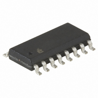
IC SWITCH QUAD SPST 16SOIC
Manufacturer
Intersil
Type
Analog Switchr
Datasheet
1.DG411DYZ.pdf
(13 pages)
Specifications of DG411DYZ
Function
Switch
Circuit
4 x SPST - NO
On-state Resistance
35 Ohm
Voltage Supply Source
Single, Dual Supply
Voltage - Supply, Single/dual (±)
5 V ~ 44 V, ±5 V ~ 20 V
Operating Temperature
-40°C ~ 85°C
Mounting Type
Surface Mount
Package / Case
16-SOIC (0.154", 3.90mm Width)
Package
16SOIC N
Maximum On Resistance
80@10.8V Ohm
Maximum High Level Output Current
30 mA
Maximum Turn-off Time
145@±15V ns
Maximum Turn-on Time
250@12V ns
Switch Architecture
SPST
Power Supply Type
Single|Dual
Lead Free Status / RoHS Status
Lead free / RoHS Compliant
Available stocks
Company
Part Number
Manufacturer
Quantity
Price
Company:

Part Number:
DG411DYZ
Manufacturer:
Intersil
Quantity:
2 640
Part Number:
DG411DYZ
Manufacturer:
VISHAY/威世
Quantity:
20 000
Company:
Part Number:
DG411DYZ-T
Manufacturer:
Intersil
Quantity:
6 050
Part Number:
DG411DYZ-T
Manufacturer:
INTERSIL
Quantity:
20 000


Electrical Specifications
NOTES:
Test Circuits and Waveforms
V
edge of the output waveform.
NOTE: Logic input waveform is inverted for switches that have the
opposite logic sense.
POWER SUPPLY CHARACTERISTICS
Positive Supply Current, I+
Negative Supply Current, I-
Logic Supply Current, I
Ground Current, I
3. V
4. The algebraic convention whereby the most negative value is a minimum and the most positive a maximum, is used in this data sheet.
5. Typical values are for DESIGN AID ONLY, not guaranteed nor subject to production testing.
O
OUTPUT
SWITCH
SWITCH
is the steady state output with the switch on. Feedthrough via switch capacitance may result in spikes at the leading and trailing
OUTPUT
OUTPUT
SWITCH
SWITCH
LOGIC
INPUT
INPUT
IN
LOGIC
INPUT
(V01)
= input voltage to perform proper function.
V
O2
PARAMETER
FIGURE 1A. MEASUREMENTS POINTS
V
FIGURE 2A. MEASUREMENT POINTS
3V
0V
0V
V
V
S
3V
0V
0V
S1
S2
GND
0V
L
t
V
ON
50%
t
O
D
6
(Single Supply) Test Conditions: V+ = +12V, V- = 0V, V
Unless Otherwise Specified. (Continued)
90%
90%
t
V+ = 13.2V, V- = 0V
V
OFF
IN
= 0V or 5V
TEST CONDITIONS
FIGURE 2. BREAK-BEFORE-MAKE TIME
t
D
DG411, DG412, DG413
t
t
FIGURE 1. SWITCHING TIMES
90%
f
r
< 20ns
< 20ns
90%
Repeat test for all IN and S.
For load conditions, see Specifications. C
capacitance.
TEMP
LOGIC
SWITCH
INPUT
V
V
(°C)
25
85
25
85
25
85
25
85
LOGIC
INPUT
INPUT
S1
S2
= 10V
= 10V
IN
1
, IN
S
S
IN
S
1
2
L
2
1
1
(Note 4)
= 5V, V
V
MIN
L
-1
-5
-1
-5
V
-
-
-
-
FIGURE 2B. TEST CIRCUITS
O
FIGURE 1B. TEST CIRCUIT
+5V
GND
V
=
IN
L
V
= 2.4V, 0.8V (Note 3),
GND
S
+5V
V+
V-
----------------------------------- -
R
(Note 5)
-0.0001
-0.0001
0.0001
0.0001
L
TYP
+15V
-15V
+
-
-
-
-
300Ω
r
R
DS ON
R
D
D
V+
L
V-
L2
1
2
-15V
(
+15V
L
)
(Note 4)
includes fixture and stray
C
stray capacitance.
MAX
D
V
L
C
35pF
O2
1
5
1
5
1
-
-
-
-
includes fixture and
L2
300Ω
R
R
L
L1
June 20, 2007
UNITS
OUTPUT
SWITCH
FN3282.13
μA
μA
μA
μA
μA
μA
μA
μA
C
L
V
C
35pF
O1
L1
V
O
Related parts for DG411DYZ
Image
Part Number
Description
Manufacturer
Datasheet
Request
R

Part Number:
Description:
Monolithic Quad SPST CMOS Analog Switches
Manufacturer:
INTERSIL [Intersil Corporation]
Datasheet:

Part Number:
Description:
Monolithic Quad Spst Cmos Analog Switches
Manufacturer:
Intersil Corporation
Datasheet:
Part Number:
Description:
Intersil Corporation [CMOS Serial Controller Interface]
Manufacturer:
Intersil Corporation
Datasheet:
Part Number:
Description:
Manufacturer:
Intersil Corporation
Datasheet:
Part Number:
Description:
357-036-542-201 CARDEDGE 36POS DL .156 BLK LOPRO
Manufacturer:
Intersil Corporation
Datasheet:
Part Number:
Description:
1024-Word x 4-Bit LSI Static RAM
Manufacturer:
Intersil Corporation
Datasheet:
Part Number:
Description:
General Purpose NPN Transistor Arrays FN341.4
Manufacturer:
Intersil Corporation
Datasheet:
Part Number:
Description:
CMOS 16-Bit Microprocessor
Manufacturer:
Intersil Corporation
Datasheet:
Part Number:
Description:
Manufacturer:
Intersil Corporation
Datasheet:
Part Number:
Description:
Manufacturer:
Intersil Corporation
Datasheet:
Part Number:
Description:
Manufacturer:
Intersil Corporation
Datasheet:
Part Number:
Description:
Manufacturer:
Intersil Corporation
Datasheet:
Part Number:
Description:
CMOS 6-Bit Latch and Decoder Memory Interfaces
Manufacturer:
Intersil Corporation
Datasheet:
Part Number:
Description:
CA3046General Purpose NPN Transistor Arrays
Manufacturer:
Intersil Corporation
Datasheet:
Part Number:
Description:
Manufacturer:
Intersil Corporation
Datasheet: