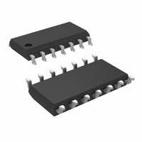
LMH6574MA/NOPB National Semiconductor, LMH6574MA/NOPB Datasheet - Page 11

LMH6574MA/NOPB
Manufacturer Part Number
LMH6574MA/NOPB
Description
IC VIDEO MULTIPLEXER 4X1 14SOIC
Manufacturer
National Semiconductor
Datasheet
1.LMH6574MANOPB.pdf
(14 pages)
Specifications of LMH6574MA/NOPB
Function
Video Multiplexer
Circuit
1 x 4:1
Voltage Supply Source
Single, Dual Supply
Voltage - Supply, Single/dual (±)
6 V ~ 12 V, ±3 V ~ 6 V
Current - Supply
13mA
Operating Temperature
-40°C ~ 85°C
Mounting Type
Surface Mount
Package / Case
14-SOIC (0.154", 3.90mm Width)
For Use With
LMH730276 - EVAL BOARD FOR HS 4:1 MUX
Lead Free Status / RoHS Status
Lead free / RoHS Compliant
Other names
*LMH6574MA
*LMH6574MA/NOPB
LMH6574MA
*LMH6574MA/NOPB
LMH6574MA
Application Notes
The LMH6574 has a current feedback output buffer with gain
determined by external feedback (R
resistors. With current feedback amplifiers, the closed loop
frequency response is a function of R
the recommended value of R
the chart “Suggested R
from the recommended value will peak the frequency re-
sponse and extend the bandwidth while increasing the value
of R
Reducing the value of R
value will cause overshoot, ringing and, eventually, oscilla-
tion.
Since all applications are slightly different it is worth some
experimentation to find the optimal R
more information see Application Note OA-13 which de-
scribes the relationship between R
quency response for current feedback operational amplifiers.
The impedance looking into pin 12 is approximately 20Ω.
This allows for good bandwidth at gains up to 10 V/V. When
used with gains over 10 V/V, the LMH6574 will exhibit a “gain
bandwidth product” similar to a typical voltage feedback
amplifier. For gains of over 10 V/V consider selecting a high
performance video amplifier like the LMH6720 to provide
additional gain.
SD vs. EN
The LMH6574 has both shutdown and disable capability.
The shutdown feature affects the entire chip, whereas the
F
will cause the frequency response to roll off faster.
F
F
vs Gain”. Generally, lowering R
too far below the recommended
F
is 575Ω. For other gains see
(Continued)
F
F
F
F
for a given circuit. For
) and gain set (R
. For a gain of 2 V/V,
and closed-loop fre-
FIGURE 3. 8:1 MUX USING TWO LMH6574’s
G
F
)
11
disable function only affects the output buffer. When in shut-
down mode, minimal power is consumed. The shutdown
function is very fast, but causes a very brief spike of about
400 mV to appear on the output. When in shutdown mode
the LMH6574 consumes only 1.8 mA of supply current. For
maximum input to output isolation use the shutdown func-
tion.
The EN pin only disables the output buffer which results in a
substantially reduced output glitch of only 50 mV. While
disabled the chip consumes 4.7 mA, considerably more than
when shutdown. This is because the input buffers are still
active. For minimal output glitch use the EN pin. Also, care
should be taken to ensure that, while in the disabled state,
the voltage differential between the active input buffer (the
one selected by pins A0 and A1) and the output pin stays
less than 2V. As the voltage differential increases, input to
output isolation decreases. Normally this is not an issue. See
the section on MULTIPLEXER EXPANSION for further de-
tails.
To reduce the output glitch when using the SD pin, switch the
EN pin at least 10 ns before switching the SD pin. This can
be accomplished by using an RC delay circuit between the
two pins if only one control signal is available.
Logic inputs "SD" and "EN" will revert to the "High", while
"A
MULITPLEXER EXPANSION
Figure 3 shows an 8:1 MUX using two LMH6574’s.
0
" and "A
1
" will revert to the "Low" state when left floating.
20119718
www.national.com


