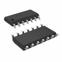
LMH6574MA/NOPB National Semiconductor, LMH6574MA/NOPB Datasheet - Page 12

LMH6574MA/NOPB
Manufacturer Part Number
LMH6574MA/NOPB
Description
IC VIDEO MULTIPLEXER 4X1 14SOIC
Manufacturer
National Semiconductor
Datasheet
1.LMH6574MANOPB.pdf
(14 pages)
Specifications of LMH6574MA/NOPB
Function
Video Multiplexer
Circuit
1 x 4:1
Voltage Supply Source
Single, Dual Supply
Voltage - Supply, Single/dual (±)
6 V ~ 12 V, ±3 V ~ 6 V
Current - Supply
13mA
Operating Temperature
-40°C ~ 85°C
Mounting Type
Surface Mount
Package / Case
14-SOIC (0.154", 3.90mm Width)
For Use With
LMH730276 - EVAL BOARD FOR HS 4:1 MUX
Lead Free Status / RoHS Status
Lead free / RoHS Compliant
Other names
*LMH6574MA
*LMH6574MA/NOPB
LMH6574MA
*LMH6574MA/NOPB
LMH6574MA
www.national.com
Application Notes
If it is important in the end application to make sure that no
two inputs are presented to the output at the same time, an
optional delay block can be added, to drive the SHUTDOWN
pin of each device. Figure 4 shows one possible approach to
this delay circuit. The delay circuit shown will delay SHUT-
DOWN’s H to L transitions (R
its L to H transition. R
in order to not reduce the SHUTDOWN voltage and to
produce little or no delay to SHUTDOWN.
With the SHUTDOWN pin putting the output stage into a
high impedance state, several LMH6574’s can be tied to-
gether to form a larger input MUX. However, there is a
loading effect on the active output caused by the unselected
devices. The circuit in Figure 5 shows how to compensate
for this effect. For the 16:1 MUX function shown in Figure 5
below the gain error would be about −0.8 dB, or about 9%. In
the circuit in Figure 5, resistor ratios have been adjusted to
compensate for this gain error. By adjusting the gain of each
multiplexer circuit the error can be reduced to the tolerance
of the resistors used (1% in this example).
Disabling of the LMH6574 using the EN pin is not recom-
mended for use when doing multiplexer expansion. While
disabled, If the voltage between the selected input and the
chip output exceeds approximately 2V the device will begin
to enter a soft breakdown state. This will show up as reduced
input to output isolation. The signal on the non-inverting
input of the output driver amplifier will leak through to the
inverting input, and then to the output through the feedback
resistor. The worst case is a gain of 1 configuration where
the non inverting input follows the active input buffer and
(through the feedback resistor) the inverting input follows the
voltage driving the output stage. The solution for this is to
use shutdown mode for multiplexer expansion.
FIGURE 5. Multiplexer Gain Compensation
FIGURE 4. Delay Circuit Implementation
2
should be kept small compared to R
1
and C
(Continued)
1
decay) but won’t delay
20119719
20119717
1
12
Other Applications
The LMH6574 could support a multi antenna receiver with
up to four separate antennas. Monitoring the signal strength
of all 4 antennas and connecting the strongest signal to the
final IF stage would provide effective spacial diversity.
For direction finding, the LMH6574 could be used to provide
high speed sampling of four separate antennas to a single
DSP which would use the information to calculate the direc-
tion of the received signal.
DRIVING CAPACITIVE LOADS
Capacitive output loading applications will benefit from the
use of a series output resistor R
of a series output resistor, R
output under capacitive loading. Capacitive loads of
5 to 120 pF are the most critical, causing ringing, frequency
response peaking and possible oscillation. The chart “Sug-
gested R
selecting a series output resistor for mitigating capacitive
loads. The values suggested in the charts are selected for
0.5 dB or less of peaking in the frequency response. This
gives a good compromise between settling time and band-
width. For applications where maximum frequency response
is needed and some peaking is tolerable, the value of R
can be reduced slightly from the recommended values.
FIGURE 7. Suggested R
FIGURE 6. Decoupling Capacitive Loads
OUT
vs. Cap Load” gives a recommended value for
OUT
OUT
OUT
, to stabilize the amplifier
vs. Capacitive Load
. Figure 6 shows the use
20119724
20119715
OUT


