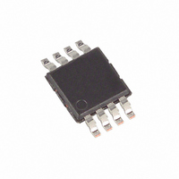
MAX4564EUA+ Maxim Integrated Products, MAX4564EUA+ Datasheet - Page 2

MAX4564EUA+
Manufacturer Part Number
MAX4564EUA+
Description
IC SWITCH SPDT 8UMAX
Manufacturer
Maxim Integrated Products
Type
Analog Switchr
Datasheet
1.MAX4564EUA.pdf
(12 pages)
Specifications of MAX4564EUA+
Function
Switch
Circuit
1 x SPDT
On-state Resistance
60 Ohm
Voltage Supply Source
Single, Dual Supply
Voltage - Supply, Single/dual (±)
1.8 V ~ 12 V, ±1.8 V ~ 6 V
Current - Supply
1µA
Operating Temperature
-40°C ~ 85°C
Mounting Type
Surface Mount
Package / Case
8-TSSOP, 8-MSOP (0.118", 3.00mm Width)
Package
8uMAX
Maximum On Resistance
275@2.7V Ohm
Maximum Propagation Delay Bus To Bus
70@±6V|100@6V ns
Maximum Low Level Output Current
20 mA
Maximum Turn-off Time
110@3.3V ns
Maximum Turn-on Time
250@3.3V ns
Switch Architecture
SPDT
Power Supply Type
Single|Dual
Lead Free Status / RoHS Status
Lead free / RoHS Compliant
ABSOLUTE MAXIMUM RATINGS
(Voltages Referenced to GND)
V+ ..........................................................................-0.3V to +13V
V- ...........................................................................-13V to +0.3V
V+ to V- ..................................................................-0.3V to +13V
EN, IN, COM, NC, NO (Note 1) .......... (V- - 0.3V) to (V+ + 0.3V)
Continuous Current (any terminal)................................... ±20mA
Peak Current, COM, NC, NO
ESD per Method 3015.7...................................................... >2kV
Low-Voltage, Dual-Supply,
SPDT Analog Switch with Enable
ELECTRICAL CHARACTERISTICS—±5V Supply
(V+ = +4.5V to +6V, V- = -4.5V to -6V, V
are at T
Note 1: Signals on NO, NC, COM, IN, or EN exceeding V+ or V- are clamped by internal diodes. Limit forward-diode current to maximum
current rating.
Stresses beyond those listed under “Absolute Maximum Ratings” may cause permanent damage to the device. These are stress ratings only, and functional
operation of the device at these or any other conditions beyond those indicated in the operational sections of the specifications is not implied. Exposure to
absolute maximum rating conditions for extended periods may affect device reliability.
2
ANALOG SWITCH
Analog Signal Range
On-Resistance
On-Resistance Match Between
Channels (Note 4)
On-Resistance Flatness
(Note 5)
NO or NC Off-Leakage Current
COM Off-Leakage Current
COM On-Leakage Current
(pulsed at 1ms, 10% duty cycle)................................ ±30mA
_______________________________________________________________________________________
A
= +25°C.) (Notes 2, 3)
PARAMETER
I
R
I
SYMBOL
V
NC(OFF)
I
COM(OFF)
I
COM(ON)
FLAT(ON)
NO(OFF)
NO
V
R
COM
R
IH
ON
, V
ON
= +2.4V, V
NC
,
or
V+ = +4.5V, V- = -4.5V,
I
V+ = +4.5V, V- = -4.5V,
I
V+ = +4.5V, V- = -4.5V, I
1mA; V
V+ = +5.5V, V- = -5.5V;
V
V
V+ = +5.5V, V- = -5.5V;
V
V
V+ = +5.5V, V- = -5.5V, V
+4.5V, -4.5V; V
-4.5V, or floating
COM
COM
COM
NO
COM
NO
IL
, V
, V
= 1mA; V
= 1mA; V
= +0.8V, GND = 0, T
= +4.5V, -4.5V;
= +4.5V, -4.5V;
NC
NC
NO
CONDITIONS
= -4.5, +4.5V
= -4.5, +4.5V
, V
NC
NO
NO
NO
= -3.5V, 0, +3.5V
, V
, V
, V
Continuous Power Dissipation (T
Operating Temperature Range
Junction Temperature .....................................................+150°C
Storage Temperature Range ............................-65°C to +150°C
Lead Temperature (soldering, 10s) ................................+300°C
NC
NC
NC
8-Pin SOT23 (derate 7.1mW/°C above +70°C) ..........571mW
8-Pin µMAX (derate 4.10mW/°C above +70°C) .........330mW
MAX4564E_A .................................................-40°C to +85°C
= ±3.5V
= ±3.5V
COM
= +4.5V,
COM
A
= T
=
=
MIN
to T
+25 C
+25 C
+25 C
+25 C
+25 C
+25 C
T
MAX
E
E
E
E
E
E
A
, unless otherwise noted. Typical values
MIN
-10
V-
-1
-5
-1
-5
-2
A
= +70°C)
TYP
0.75
0.05
0.05
0.05
6.5
40
MAX
100
V+
60
10
13
10
3
4
1
5
1
5
2
UNITS
nA
nA
nA
V


