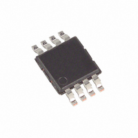
MAX4564EUA+ Maxim Integrated Products, MAX4564EUA+ Datasheet - Page 8

MAX4564EUA+
Manufacturer Part Number
MAX4564EUA+
Description
IC SWITCH SPDT 8UMAX
Manufacturer
Maxim Integrated Products
Type
Analog Switchr
Datasheet
1.MAX4564EUA.pdf
(12 pages)
Specifications of MAX4564EUA+
Function
Switch
Circuit
1 x SPDT
On-state Resistance
60 Ohm
Voltage Supply Source
Single, Dual Supply
Voltage - Supply, Single/dual (±)
1.8 V ~ 12 V, ±1.8 V ~ 6 V
Current - Supply
1µA
Operating Temperature
-40°C ~ 85°C
Mounting Type
Surface Mount
Package / Case
8-TSSOP, 8-MSOP (0.118", 3.00mm Width)
Package
8uMAX
Maximum On Resistance
275@2.7V Ohm
Maximum Propagation Delay Bus To Bus
70@±6V|100@6V ns
Maximum Low Level Output Current
20 mA
Maximum Turn-off Time
110@3.3V ns
Maximum Turn-on Time
250@3.3V ns
Switch Architecture
SPDT
Power Supply Type
Single|Dual
Lead Free Status / RoHS Status
Lead free / RoHS Compliant
Low-Voltage, Dual-Supply,
SPDT Analog Switch with Enable
The MAX4564 is a dual-supply SPDT CMOS analog
switch. The MAX4564 has break-before-make switch-
ing. The CMOS switch construction provides Rail-to-
Rail
power. Each of the two switches is independently con-
trolled by a TTL/CMOS-level-compatible digital input.
Do not exceed the absolute maximum ratings because
stresses beyond the listed ratings may cause perma-
nent damage to the device. Proper power-supply
sequencing is recommended for all CMOS devices.
Always sequence V+ on first, then V-, followed by the
logic inputs NO, NC, or COM. If power-supply
sequencing is not possible, add two small-signal
diodes (D1, D2) in series with supply pins. Adding
diodes reduces the analog signal range to one diode
drop below V+ and one diode drop above V-, but does
not affect the device’s low switch resistance and low
leakage characteristics.
Rail-to-Rail is a registered trademark of Nippon Motorola, Ltd.
8
_______________________________________________________________________________________
®
MAX
1
2
3
4
5
6
7
8
signal handling while consuming virtually no
Applications Information
SOT23
8
7
6
5
3
4
1
2
Detailed Description
Overvoltage Protection
NAME
COM
GND
NO
EN
NC
V+
IN
V-
Analog Switch Common
Device Enable. Drive EN low for normal SPDT switch operation. If EN is high, both
NO and NC are disconnected.
Negative Supply Voltage
Ground
Digital Control Input
Analog Switch Normally Open
Analog Switch Normally Closed
Positive Supply Voltage
Figure 1. Overvoltage Protection Using Two External Blocking
Diodes
V g
FUNCTION
NO
POSITIVE SUPPLY
NEGATIVE SUPPLY
V-
V+
Timing Diagrams
D1
D2
Pin Description
COM
Test Circuits/
MAX4564


