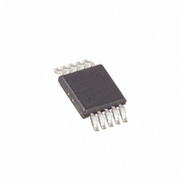
MAX4634EUB+ Maxim Integrated Products, MAX4634EUB+ Datasheet - Page 5

MAX4634EUB+
Manufacturer Part Number
MAX4634EUB+
Description
IC MULTIPLEXER 4X1 10UMAX
Manufacturer
Maxim Integrated Products
Datasheet
1.MAX4634ETBT.pdf
(10 pages)
Specifications of MAX4634EUB+
Function
Multiplexer
Circuit
1 x 4:1
On-state Resistance
4 Ohm
Voltage Supply Source
Single Supply
Voltage - Supply, Single/dual (±)
1.8 V ~ 5.5 V
Current - Supply
0.001µA
Operating Temperature
-40°C ~ 85°C
Mounting Type
Surface Mount
Package / Case
10-MSOP, Micro10™, 10-uMAX, 10-uSOP
Product
Multiplexer
Number Of Lines (input / Output)
4.0 / 1.0
Supply Voltage (max)
5.5 V
Supply Voltage (min)
1.8 V
Maximum Operating Temperature
+ 85 C
Minimum Operating Temperature
- 40 C
Mounting Style
SMD/SMT
Number Of Input Lines
4.0
Number Of Output Lines
1.0
Power Dissipation
330 mW
Lead Free Status / RoHS Status
Lead free / RoHS Compliant
ELECTRICAL CHARACTERISTICS—Single +3V Supply (continued)
(V+ = +2.7V to +3.3V, V
T
Note 2: The algebraic convention, where the most negative value is a minimum and the most positive value a maximum, is used in
Note 3: TDFN parts are tested at +25°C and guaranteed by design and correlation over the entire temperature range.
Note 4: ΔR
Note 5: R
Note 6: Flatness is defined as the difference between the maximum and minimum value of on-resistance as measured over the
Note 7: Guaranteed by design.
Note 8: Off-isolation = 20log
Note 9: Between any two switches.
(T
A
POWER SUPPLY
NO_ Off-Capacitance
COM Off-Capacitance
COM On-Capacitance
Total Harmonic Distortion
Positive Supply Current
A
= +25°C.) (Notes 2, 3)
= +25°C, unless otherwise noted.)
20
15
10
5
0
0
this data sheet.
specified analog signal ranges.
PARAMETER
ON
ON
ON-RESISTANCE vs. V
and ΔR
1
= R
ON(MAX)
V+ = 2.5V
V+ = 1.8V
_______________________________________________________________________________________
2
ON
V
V+ = 3.0V
COM
matching specifications for TDFN-packaged parts are guaranteed by design.
IH
(V)
- R
3
= 2.0V, V
10
ON(MIN)
(V
COM
4-Channel CMOS Analog Multiplexer
V+ = 5.0V
C
C
COM
4
SYMBOL
NO_(OFF)
COM(OFF)
C
THD
(ON)
I+
.
IL
/ V
5
= 0.4V, T
NO
), where V
V
V
V
R
V+ = 3.3V, V
5.0
4.5
4.0
3.5
3.0
2.5
NO_
COM
COM
L
= 600Ω, f = 20Hz to 20kHz
A
0
= -40°C to +85°C, unless otherwise noted. Typical values are at V+ = +3V,
= GND, f = 1MHz, Figure 6
= GND, f = 1MHz, Figure 6
= V
COM
T
ON-RESISTANCE vs. V
A
0.5
NO_
= -40°C
TEMPERATURE (V+ = +3V)
= output and V
IH
= GND, f = 1MHz, Figure 6
1.0
= V+, V
CONDITIONS
V
COM
T
A
1.5
= +85°C
(V)
IL
Fast, Low-Voltage, 4 Ω ,
T
Typical Operating Characteristics
A
= 0
= +25°C
2.0
NO
COM
= input to off switch.
AND
2.5
3.0
4.0
3.5
3.0
2.5
2.0
1.5
0
MIN
T
A
ON-RESISTANCE vs. V
= +25°C
TEMPERATURE (V+ = +5V)
1
0.018
0.001
TYP
13
52
68
2
V
T
COM
A
= +85°C
(V)
3
MAX
1
COM
T
A
AND
4
= -40°C
UNITS
µA
pF
pF
pF
%
5
5


