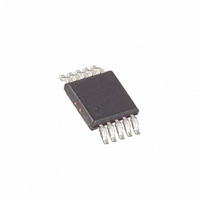
MAX4634EUB+ Maxim Integrated Products, MAX4634EUB+ Datasheet - Page 7

MAX4634EUB+
Manufacturer Part Number
MAX4634EUB+
Description
IC MULTIPLEXER 4X1 10UMAX
Manufacturer
Maxim Integrated Products
Datasheet
1.MAX4634ETBT.pdf
(10 pages)
Specifications of MAX4634EUB+
Function
Multiplexer
Circuit
1 x 4:1
On-state Resistance
4 Ohm
Voltage Supply Source
Single Supply
Voltage - Supply, Single/dual (±)
1.8 V ~ 5.5 V
Current - Supply
0.001µA
Operating Temperature
-40°C ~ 85°C
Mounting Type
Surface Mount
Package / Case
10-MSOP, Micro10™, 10-uMAX, 10-uSOP
Product
Multiplexer
Number Of Lines (input / Output)
4.0 / 1.0
Supply Voltage (max)
5.5 V
Supply Voltage (min)
1.8 V
Maximum Operating Temperature
+ 85 C
Minimum Operating Temperature
- 40 C
Mounting Style
SMD/SMT
Number Of Input Lines
4.0
Number Of Output Lines
1.0
Power Dissipation
330 mW
Lead Free Status / RoHS Status
Lead free / RoHS Compliant
The MAX4634 is a low-on-resistance, low-voltage ana-
log multiplexer that operates from a +1.8V to +5.5V sin-
gle supply. CMOS switch construction allows pro-
cessing of analog signals that are within the supply volt-
age range (GND to V+).
To disable all switch channels, drive EN low. All four inputs
and COM become high impedance during this state. If the
disable feature is not needed, connect EN to V+.
µMAX/
TDFN
PIN
10
—
1
2
3
4
5
6
7
8
9
NAME
COM
GND
NO1
NO3
NO4
NO2
EN
V+
A0
A1
EP
_______________________________________________________________________________________
Detailed Description
Address Input. See the Truth Table
for details.
Normally Open Switch 1
Ground
Normally Open Switch 3
Enable Logic Input. See the Truth
Table for details.
Positive Supply Voltage. Connect
to an external power supply.
Bypass to GND with a 10µF
capacitor placed as close to the
pin as possible.
Normally Open Switch 4
Analog Switch Common Terminal
Normally Open Switch 2
Address Input. See the Truth Table
for details.
Exposed Pad. Internally connected
to GND. Connect to a large PCB
ground plane for proper operation.
Not intended as an electrical
connection point (TDFN package
only).
4-Channel CMOS Analog Multiplexer
Pin Description
FUNCTION
Figure 1. Overvoltage Protection Using External Blocking Diodes
Proper power-supply sequencing is recommended for
all CMOS devices. Always apply V+ before applying
analog signals or logic inputs, especially if the analog or
logic signals are not current limited. If this sequencing is
not possible, and if the analog or logic inputs are not
current limited to < 20mA, add a small-signal diode
(D1) as shown in Figure 1. If the analog signal can dip
below GND, add D2. Adding protection diodes reduces
the analog signal range to a diode drop (about 0.7V)
below V+ for D1 or to a diode drop above ground for D2.
The addition of diodes does not affect leakage. On-resis-
tance increases by a small amount at low supply voltages.
Maximum supply voltage (V+) must not exceed 6V.
Protection diodes D1 and D2 also protect against some
overvoltage situations. A fault voltage up to the
absolute maximum rating at an analog signal input
does not damage the device, even if the supply voltage
is below the signal voltage.
Fast, Low-Voltage, 4 Ω ,
COM
Applications Information
Power-Supply Sequencing and
GND
*
*
V+
Overvoltage Protection
+5V
D1
D2
*INTERNAL PROTECTION DIODES
*
*
MAX4634
NO
7


