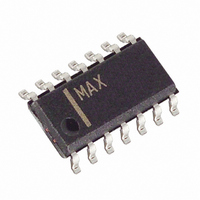
MAX4535ESD+ Maxim Integrated Products, MAX4535ESD+ Datasheet - Page 10

MAX4535ESD+
Manufacturer Part Number
MAX4535ESD+
Description
IC MULTIPLEXER DUAL 2X1 14SOL
Manufacturer
Maxim Integrated Products
Datasheet
1.MAX4535ESD.pdf
(14 pages)
Specifications of MAX4535ESD+
Function
Multiplexer
Circuit
2 x 2:1
On-state Resistance
400 Ohm
Voltage Supply Source
Single, Dual Supply
Voltage - Supply, Single/dual (±)
9 V ~ 36 V, ±4.5 V ~ 20 V
Operating Temperature
-40°C ~ 85°C
Mounting Type
Surface Mount
Package / Case
14-SOIC (0.154", 3.90mm Width)
Lead Free Status / RoHS Status
Lead free / RoHS Compliant
The maximum allowable input voltage for safe opera-
tion depends on whether supplies are on or off and on
the load configuration at the COM output. If COM is
referred to a voltage other than ground, but within the
supplies, VNO_ may range higher or lower than the
supplies, provided the absolute value of VNO_ -
VCOM_ is less than 40V. For example, if the load is
referred to +10V at COM_, then the NO_ voltage range
can be from +50V to -30V. As another example, if the
load is connected to -10V at COM_, the NO_ voltage
range is limited to -50V to +30V.
If the supplies are ±15V and COM is referenced to
ground through a load, the maximum NO_ voltage is
±36V. If the supplies are off and the COM output is ref-
erenced to ground, the maximum NO_ voltage is ±40V.
Two comparators continuously compare the voltage on
the NO_ pin with V+ and V- supply voltages. When the
signal on NO_ is between V+ and V-, the multiplexer
behaves normally, with FETs N1 and P1 turning on and
Fault-Protected, High-Voltage,
Single 4-to-1/Dual 2-to-1 Multiplexers
Figure 1. Functional Diagram
10
______________________________________________________________________________________
GND
NO_
V+
A_
V-
ESD DIODE
NO_ Input Voltage
Normal Operation
NORMALLY OPEN SWITCH CONSTRUCTION
FAULT
FAULT
HIGH
LOW
ON
off in response to A_ signals (Figure 1). The parallel
combination of N1 and P1 forms a low-value resistor
between NO_ and COM_ so that signals pass equally
well in either direction.
When the signal on NO_ exceeds V+ by about 150mV,
the positive fault comparator output goes high, turning
off FETs N1 and P1 (Figure 1). This makes the NO_ pin
high impedance regardless of the switch state. If the
switch state is “off,” all FETs turn off, and both NO_ and
COM_ are high impedance. If the switch state is “on,”
FET P2 turns on, clamping COM_ to V+.
When the signal on NO_ goes about 150mV below V-,
the negative fault comparator output goes high, turning
off FETs N1 and P1 (Figure 1). This makes the NO pin
high impedance regardless of the switch state. If the
switch state is “off,” all FETs turn off, and both NO_ and
COM_ are high impedance. If the switch state is “on,”
FET N2 turns on, clamping COM_ to V-.
N1
Negative Fault Condition
Positive Fault Condition
P1
MAX4534
MAX4535
P2
N2
COM_


