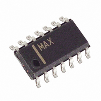
MAX4535ESD+ Maxim Integrated Products, MAX4535ESD+ Datasheet - Page 9

MAX4535ESD+
Manufacturer Part Number
MAX4535ESD+
Description
IC MULTIPLEXER DUAL 2X1 14SOL
Manufacturer
Maxim Integrated Products
Datasheet
1.MAX4535ESD.pdf
(14 pages)
Specifications of MAX4535ESD+
Function
Multiplexer
Circuit
2 x 2:1
On-state Resistance
400 Ohm
Voltage Supply Source
Single, Dual Supply
Voltage - Supply, Single/dual (±)
9 V ~ 36 V, ±4.5 V ~ 20 V
Operating Temperature
-40°C ~ 85°C
Mounting Type
Surface Mount
Package / Case
14-SOIC (0.154", 3.90mm Width)
Lead Free Status / RoHS Status
Lead free / RoHS Compliant
X = Don’t care; logic 0: V
MAX4535 (Dual 2-to-1 Mux)
X = Don’t care; logic 0: V
The MAX4534/MAX4535 differ considerably from tradi-
tional fault-protected multiplexers, offering several
advantages. First, they are constructed with two paral-
lel FETs, allowing very low resistance when the switch
is on. Second, they allow signals on the NO_ pins that
are within or beyond the supply rails to be passed
through the switch to the COM terminal. This allows rail-
MAX4534 (Single 4-to-1 Mux)
MAX4534 (Single 4-to-1 Mux)
6, 8, 9
PIN
A1
A0
10
11
12
13
14
X
0
0
1
1
X
0
1
1
2
3
4
5
7
NAME
A0
EN
COM
GND
X
0
1
0
1
0
1
1
NO1
NO2
N.C.
NO4
NO3
EN
V+
A0
A1
V-
_______________________________________________________________________________________
EN
0
1
1
1
1
Address Bit 0
Enable Input
Negative Supply Voltage
Channel Input 1 (fault protected)
Channel Input 2 (fault protected)
No connection
Analog Output
Channel Input 4 (fault protected)
Channel Input 3 (fault protected)
Positive Supply Voltage
Ground
Address Bit 1
AL
AL
COMA
Detailed Description
NO1A
NO2A
None
≤ +0.8; logic 1: V
≤ +0.8; logic 1: V
Single 4-to-1/Dual 2-to-1 Multiplexers
FUNCTION
ON SWITCH
Truth Tables
None
NO1
NO2
NO3
NO4
AH
AH
COMB
Fault-Protected, High-Voltage,
NO1B
NO2B
≥ +2.4V
None
≥ +2.4V
to-rail signal operation. Third, when a signal on VNO_
exceeds the supply rails (i.e., a fault condition), the
voltage on COM_ is limited to the supply rails.
Operation is identical for both fault polarities.
When the NO_ voltage goes beyond supply rails (fault
condition), the NO_ input becomes high impedance
regardless of the switch state or load resistance. When
power is removed, and the fault protection is still in
effect, the NO_ terminals are a virtual open circuit. The
fault can be up to ±40V, with V+ = V- = 0. If the switch
is on, the COM_ output current is furnished from the V+
or V- pin by “booster” FETs connected to each supply
pin. These FETs can source or sink up to 10mA.
The COM_ pins are not fault-protected. If a voltage
source is connected to any COM_ pin, it should be lim-
ited to the supply voltages. Exceeding the supply volt-
age will cause high currents to flow through the ESD
protection diodes, damaging the device (see Absolute
Maximum Ratings).
Figure 1 shows the internal construction, with the ana-
log signal paths shown in bold. A single, normally open
(NO) switch is shown. The analog switch is formed by
the parallel combination of N-channel FET N1 and P-
channel FET P1, which are driven on and off simultane-
ously, according to the input fault condition and the
logic level state.
.
MAX4535 (Dual 2-to-1 Mux)
6, 9, 14
PIN
10
11
12
13
1
2
3
4
5
7
8
COMA
COMB
NAME
NO1A
NO2A
NO2B
NO1B
GND
N.C.
EN
A0
V+
V-
Address Bit 0
Enable Input
Negative Supply Voltage
Channel Input 1A (fault protected)
Channel Input 2A (fault protected)
No connection
Mux Output A
Mux Output B
Channel Input 2B (fault protected)
Channel Input 1B (fault protected)
Positive Supply Voltage
Ground
Pin Descriptions
FUNCTION
9


