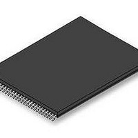
S29GL128S10TFI010 Spansion Inc., S29GL128S10TFI010 Datasheet - Page 40

S29GL128S10TFI010
Manufacturer Part Number
S29GL128S10TFI010
Description
Flash 128 MBIT 3V 100NS PAGE MODE FLASH
Manufacturer
Spansion Inc.
Datasheet
1.S29GL128S10TFI010.pdf
(97 pages)
Specifications of S29GL128S10TFI010
Data Bus Width
16 bit
Memory Type
Flash
Memory Size
128 Mbit
Architecture
Uniform
Timing Type
Asynchronous
Interface Type
CFI
Access Time
100 ns
Supply Voltage (max)
3.6 V
Supply Voltage (min)
2.7 V
Maximum Operating Current
100 mA
Operating Temperature
- 40 C to + 85 C
Mounting Style
SMD/SMT
Package / Case
TSOP-56
Lead Free Status / Rohs Status
Compliant
Available stocks
Company
Part Number
Manufacturer
Quantity
Price
Part Number:
S29GL128S10TFI010
Manufacturer:
SPANSIO
Quantity:
20 000
D a t a
S h e e t
( A d v a n c e
I n f o r m a t i o n )
5.4.3
Data Polling Status
During an active Embedded Algorithm the EAC switches to the Data Polling ASO to display EA status to any
read access. A single word of status information is aliased in all locations of the device address space. In the
status word there are several bits to determine the status of an EA. These are referred to as DQ bits as they
appear on the data bus during a read access while an EA is in progress. DQ bits 15 to 8, DQ4, and DQ0 are
reserved and provide undefined data. Status monitoring software must mask the reserved bits and treat them
as don't care.
Table 5.5 on page 44
and the following subsections describe the functions of the remaining
bits.
Note that in future technology nodes the Data Polling Status feature will not be supported. The user is
strongly advised to use the Status Register to determine device status.
5.4.3.1
DQ7: Data# Polling
The Data# Polling bit, DQ7, indicates to the host system whether an Embedded Algorithm is in progress or
has completed. Data# Polling is valid after the rising edge of the final WE# pulse in the program or erase
command sequence. Note that the Data# Polling is valid only for the last word being programmed in the write-
buffer-page during Write Buffer Programming. Reading Data# Polling status on any word other than the last
word to be programmed in the write-buffer-page will return false status information.
During the Embedded Program algorithm, the device outputs on DQ7 the complement of the data bit
programmed to DQ7. This DQ7 status also applies to programming during Erase Suspend. When the
Embedded Program algorithm is complete, the device outputs the data bit programmed to bit 7 of the last
word programmed. In case of a Program Suspend, the device allows only reading array data. If a program
address falls within a protected sector, Data# Polling on DQ7 is active for approximately 20 µs, then the
device returns to reading array data.
During the Embedded Erase or blank check algorithms, Data# Polling produces a 0 on DQ7. When the
algorithm is complete, or if the device enters the Erase Suspend mode, Data# Polling produces a '1' on DQ7.
This is analogous to the complement / true datum output described for the Embedded Program algorithm: the
erase function changes all the bits in a sector to '1'; prior to this, the device outputs the complement or '0'. The
system must provide an address within the sector selected for erasure to read valid status information on
DQ7.
After an erase command sequence is written, if the sector selected for erasing is protected, Data# Polling on
DQ7 is active for approximately 100 µs, then the device returns to reading array data.
When the system detects DQ7 has changed from the complement to true data, it can read valid data at
DQ15-DQ0 on the following read cycles. This is because DQ7 may change asynchronously with DQ6-DQ0
while Output Enable (OE#) is asserted Low. This is illustrated in
Figure 10.15 on page
85.
Table 5.5
on page 44
shows the outputs for Data# polling on DQ7.
Figure 5.2 on page 30
shows the Data# polling
algorithm use in Write Buffer Programming.
Valid DQ7 data polling status may only be read from:
the address of the last word loaded into the Write Buffer for a Write Buffer programming operation;
the location of a single word programming operation;
or a location in a sector being erased or blank checked.
®
40
GL-S MirrorBit
Family
S29GL_128S_01GS_00_01 February 11, 2011


