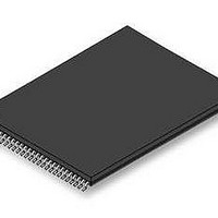
S29GL128S10TFI010 Spansion Inc., S29GL128S10TFI010 Datasheet - Page 59

S29GL128S10TFI010
Manufacturer Part Number
S29GL128S10TFI010
Description
Flash 128 MBIT 3V 100NS PAGE MODE FLASH
Manufacturer
Spansion Inc.
Datasheet
1.S29GL128S10TFI010.pdf
(97 pages)
Specifications of S29GL128S10TFI010
Data Bus Width
16 bit
Memory Type
Flash
Memory Size
128 Mbit
Architecture
Uniform
Timing Type
Asynchronous
Interface Type
CFI
Access Time
100 ns
Supply Voltage (max)
3.6 V
Supply Voltage (min)
2.7 V
Maximum Operating Current
100 mA
Operating Temperature
- 40 C to + 85 C
Mounting Style
SMD/SMT
Package / Case
TSOP-56
Lead Free Status / Rohs Status
Compliant
Available stocks
Company
Part Number
Manufacturer
Quantity
Price
Part Number:
S29GL128S10TFI010
Manufacturer:
SPANSIO
Quantity:
20 000
Legend:
X = Don't care
RA = Address of the memory to be read.
RD = Data read from location RA during read operation.
PA = Address of the memory location to be programmed.
PD = Data to be programmed at location PA.
SA = Address of the sector selected. Address bits A
WBL = Write Buffer Location. The address must be within the same Line.
WC = Word Count is the number of write buffer locations to load minus 1.
PWAx = Password address for word0 = 00h, word1 = 01h, word2 = 02h, and word3 = 03h.
PWDx = Password data word0, word1, word2, and word3.
Notes:
1. See
2. All values are in hexadecimal.
3. Except for the following, all bus cycles are write cycle: read cycle during Read, ID/CFI Read (Manufacturing ID / Device ID), Indicator Bits,
4. Data bits DQ15-DQ8 are don't care in command sequences, except for RD, PD, WC and PWD.
5. Address bits A
6. No unlock or command cycles required when reading array data.
7. The Reset command is required to return to reading array data when device is in the ID-CFI (autoselect) mode, or if DQ5 goes High
8. Command is valid when device is ready to read array data or when device is in ID-CFI (autoselect) mode.
9. The system can read and program/program suspend in non-erasing sectors, or enter the ID-CFI ASO, when in the Erase Suspend mode.
10. The Erase Resume/Program Resume command is valid only during the Erase Suspend/Program Suspend modes.
11. Issue this command sequence to return to READ mode after detecting device is in a Write-to-Buffer-Abort state. IMPORTANT: the full
12. The Exit command returns the device to reading the array.
13. The password portion can be entered or read in any order as long as the entire 64-bit password is entered or read.
February 11, 2011 S29GL_128S_01GS_00_01
Secure Silicon Region Read, SSR Lock Read, and 2nd cycle of Status Register Read .
(while the device is providing status data).
The Erase Suspend command is valid only during a sector erase operation.
command sequence is required if resetting out of ABORT.
Command Sequence
PPB Lock Entry
PPB Lock Bit Cleared
PPB Lock Status Read
(Note 17)
Command Set Exit
(Notes 12, 16)
Reset/ASO Exit
DYB ASO Entry
DYB Set
DYB Clear
DYB Status Read
(Note 17)
Command Set Exit
(Notes 12, 16)
Reset/ASO Exit
ECC Status Enter
ECC Status Read
Reset/ASO Exit
Table 8.1, Interface States on page 67
(Note 1)
(Note 17)
(Note 17)
MAX
(Note 16)
(Note 16)
-A11 are don't cares for unlock and command cycles, unless SA or PA required. (A
D a t a
3
2
1
2
1
3
2
2
1
2
1
2
1
1
Addr
XXX
XXX
XXX
XXX
XXX
XXX
XXX
XXX
XXX
555
555
555
SA
RA
S h e e t
Global Non-Volatile Sector Protection Freeze Command Set Definitions
First
for description of bus operations.
RD (0)
RD (0)
Data
RD
AA
AA
AA
A0
90
F0
A0
A0
90
F0
F0
Table 6.1 Command Definitions (Sheet 3 of 3)
MAX
Volatile Sector Protection Command Set Definitions
-A16 uniquely select any sector.
( A d v a n c e
Addr
XXX
XXX
XXX
2AA
2AA
2AA
SA
SA
Second
Data
GL-S MirrorBit
55
55
55
0
0
0
1
0
Addr
555
555
555
Third
I n f o r m a t i o n )
Data
®
E0
50
75
Family
Bus Cycles (Notes 2-5)
Addr
Fourth
Data
MAX
is the Highest Address pin.).
Addr
Fifth
Data
Addr
Sixth
Data
Addr
Seventh
Data
59


