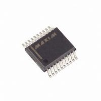
MAX4598EAP+ Maxim Integrated Products, MAX4598EAP+ Datasheet - Page 2

MAX4598EAP+
Manufacturer Part Number
MAX4598EAP+
Description
IC MULTIPLEXER DUAL 4X1 20SSOP
Manufacturer
Maxim Integrated Products
Datasheet
1.MAX4598EAP.pdf
(12 pages)
Specifications of MAX4598EAP+
Function
Multiplexer
Circuit
2 x 4:1
On-state Resistance
75 Ohm
Voltage Supply Source
Single, Dual Supply
Voltage - Supply, Single/dual (±)
2.7 V ~ 12 V, ± 2.7 V ~ 6 V
Operating Temperature
-40°C ~ 85°C
Mounting Type
Surface Mount
Package / Case
20-SSOP
Lead Free Status / RoHS Status
Lead free / RoHS Compliant
ABSOLUTE MAXIMUM RATINGS
V+ to GND ..............................................................-0.3V to +13V
V- to GND ...............................................................-13V to +0.3V
V+ to V-...................................................................-0.3V to +13V
A_, EN, LATCH, NLATCH, NO_, COM_
Continuous Current (any terminal)....................................±20mA
Peak Current, NO_, or COM_
Low-Voltage, Combination Single-Ended
8-to-1/Differential 4-to-1 Multiplexer
Note 1: Signals on NO_, COM_, EN, LATCH, NLATCH, or A_ exceeding V+ or V- are clamped by internal diodes. Limit forward cur-
Stresses beyond those listed under “Absolute Maximum Ratings” may cause permanent damage to the device. These are stress ratings only, and functional
operation of the device at these or any other conditions beyond those indicated in the operational sections of the specifications is not implied. Exposure to
absolute maximum rating conditions for extended periods may affect device reliability.
ELECTRICAL CHARACTERISTICS—Dual Supplies
(V+ = +5V ±10%, V- = -5V ±10%, V
T
2
(Note 1)...............................................(V- - 0.3V) to (V+ + 0.3V)
(pulsed at 1ms, 10% duty cycle max) ............................±40mA
LOGIC INPUTS
SWITCH
Analog Signal Range
On-Resistance
On-Resistance Matching
Between Channels (Note 4)
On-Resistance Flatness
(Note 5)
NO Off-Leakage Current
(Note 6)
COM Off-Leakage Current
(Note 6)
COM On-Leakage Current
(Note 6)
Input High Voltage
Input Low Voltage
Input Current with Input
Voltage High
Input Current with Input
Voltage Low
A
= +25°C.) (Note 2)
_______________________________________________________________________________________
rent to maximum current ratings
PARAMETER
I
SYMBOL
I
COM(OFF)
I
COM(ON)
V
NO(OFF)
R
∆R
V
COM_
R
V
FLAT
V
NO_
I
I
IH
ON
IH
IL
IH
ON
IL
= 2.4V, V
,
(Note 3)
I
V
V+ = 4.5V, V- = -4.5V
I
V
I
V
V+ = 4.5V, V- = -4.5V
V
V
V+ = 5.5V, V- = -5.5V
V
V
V+ = 5.5V, V- = -5.5V
V
V
V+ = 5.5V, V- = -5.5V
V
V
COM_
COM_
V+ = 4.5V, V- = -4.5V
COM_
NO_
NO_
NO_
NO
COM_
COM_
NO_
COM_
NO_
EN
EN
_ = ±4.5V,
= V
= V
IL
= ±3.0V,
= ±3.0V,
= -3V, 0, 3V;
= ±4.5V,
= ±4.5V,
= 1mA,
= 1mA,
= 1mA;
= ±4.5V,
= ±4.5V,
= ±4.5V,
= 0.8V, T
±
A_
A_
±
= V
= V
LATCH
LATCH
CONDITIONS
A
= T
= V
= V
Continuous Power Dissipation (T
Operating Temperature Ranges
Storage Temperature Range .............................-65°C to +160°C
Lead Temperature (soldering, 10sec) .............................+300°C
MIN
T
T
T
T
T
T
T
T
T
T
T
T
SSOP (derate 8mW/°C above +70°C) .........................640mW
Wide SO (derate 10mW/°C above +70°C)...................800mW
Plastic DIP (derate 10.53mW/°C above +70°C) ..........889mW
MAX4598C_P ......................................................0°C to +70°C
MAX4598E_P ...................................................-40°C to +85°C
NLATCH
NLATCH
A
A
A
A
A
A
A
A
A
A
A
A
= +25°C
= T
= +25°C
= T
= +25°C
= T
= +25°C
= T
= +25°C
= T
= +25°C
= T
to T
MIN
MIN
MIN
MIN
MIN
MIN
MAX
= V
= V
to T
to T
to T
to T
to T
to T
, unless otherwise noted. Typical values are at
CAL
CAL
MAX
MAX
MAX
MAX
MAX
MAX
= V+
= 0
MIN
-0.1
-0.2
-0.2
-0.1
-0.1
-10
-10
2.4
V-
-2
A
= +70°C)
TYP
0.01
0.01
0.01
0.01
0.01
1.7
1.4
45
1
7
MAX
100
0.1
0.2
0.2
0.8
0.1
0.1
V+
75
10
13
10
10
4
6
2
UNIT
nA
nA
nA
µA
µA
Ω
Ω
Ω
V
V
V


