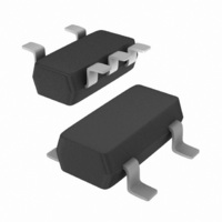
74LVC1G66GV,125 NXP Semiconductors, 74LVC1G66GV,125 Datasheet - Page 9

74LVC1G66GV,125
Manufacturer Part Number
74LVC1G66GV,125
Description
IC SWITCH SPST SC74A
Manufacturer
NXP Semiconductors
Series
74LVCr
Type
Analog Switchr
Datasheet
1.74LVC1G66GM115.pdf
(25 pages)
Specifications of 74LVC1G66GV,125
Package / Case
SC-74A, SOT-753
Function
Switch
Circuit
1 x SPST- NO
On-state Resistance
6 Ohm
Voltage Supply Source
Single Supply
Voltage - Supply, Single/dual (±)
1.65 V ~ 5.5 V
Current - Supply
0.1µA
Operating Temperature
-40°C ~ 125°C
Mounting Type
Surface Mount
Switch Configuration
SPST
On Resistance (max)
34 Ohm (Typ) @ 1.95 V
On Time (max)
5.3 ns (Typ) @ 1.95 V
Off Time (max)
4.2 ns (Typ) @ 1.95 V
Supply Voltage (max)
5.5 V
Supply Voltage (min)
1.65 V
Maximum Power Dissipation
250 mW
Maximum Operating Temperature
+ 125 C
Mounting Style
SMD/SMT
Minimum Operating Temperature
- 40 C
Switch Current (typ)
0.0001 mA @ 3.3 V
Package
5SOT-753
Maximum On Resistance
195@1.95V Ohm
Maximum Propagation Delay Bus To Bus
0.8(Typ)@1.95V|0.4(Typ)@2.7V|0.3(Typ)@3.6V|0.2(Typ)@5.5V ns
Maximum Low Level Output Current
50 mA
Maximum Turn-off Time
4.2(Typ)@1.95V ns
Maximum Turn-on Time
5.3(Typ)@1.95V ns
Switch Architecture
SPST
Power Supply Type
Single
Lead Free Status / RoHS Status
Lead free / RoHS Compliant
Lead Free Status / RoHS Status
Lead free / RoHS Compliant, Lead free / RoHS Compliant
Other names
74LVC1G66GV
74LVC1G66GV
935272034125
74LVC1G66GV
935272034125
NXP Semiconductors
11. Dynamic characteristics
Table 9.
At recommended operating conditions; voltages are referenced to GND (ground = 0 V); for test circuit see
74LVC1G66
Product data sheet
Symbol Parameter
t
t
pd
en
Fig 15. ON resistance as a function of input voltage; V
(1) T
(2) T
(3) T
(4) T
propagation delay Y to Z or Z to Y;
enable time
amb
amb
amb
amb
Dynamic characteristics
= 125 °C.
= 85 °C.
= 25 °C.
= −40 °C.
Conditions
see
E to Y or Z; see
V
V
V
V
V
V
V
V
V
V
CC
CC
CC
CC
CC
CC
CC
CC
CC
CC
Figure 16
R
(Ω)
= 1.65 V to 1.95 V
= 2.3 V to 2.7 V
= 2.7 V
= 3.0 V to 3.6 V
= 4.5 V to 5.5 V
= 1.65 V to 1.95 V
= 2.3 V to 2.7 V
= 2.7 V
= 3.0 V to 3.6 V
= 4.5 V to 5.5 V
ON
7
6
5
4
3
0
All information provided in this document is subject to legal disclaimers.
Figure 17
1
Rev. 7 — 30 July 2010
2
CC
[2][3]
[4]
(1)
(2)
(3)
(4)
= 5.0 V
3
Min
1.0
1.0
1.0
1.0
1.0
-
-
-
-
-
−40 °C to +85 °C
4
001aaa711
V
Typ
I
(V)
0.8
0.4
0.4
0.3
0.2
5.3
3.0
2.6
2.5
1.9
[1]
5
Max
2.0
1.2
1.0
0.8
0.6
6.5
6.0
5.0
4.2
12
−40 °C to +125 °C Unit
74LVC1G66
Min
1.0
1.0
1.0
1.0
1.0
-
-
-
-
-
© NXP B.V. 2010. All rights reserved.
Figure
Bilateral switch
Max
15.5
3.0
2.0
1.5
1.5
1.0
8.5
8.0
6.5
5.5
18.
ns
ns
ns
ns
ns
ns
ns
ns
ns
ns
9 of 25


