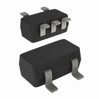
74LVC1G66GW,125 NXP Semiconductors, 74LVC1G66GW,125 Datasheet - Page 11

74LVC1G66GW,125
Manufacturer Part Number
74LVC1G66GW,125
Description
IC SWITCH SPST 5TSSOP
Manufacturer
NXP Semiconductors
Series
74LVCr
Type
Analog Switchr
Datasheet
1.74LVC1G66GM115.pdf
(25 pages)
Specifications of 74LVC1G66GW,125
Package / Case
6-TSSOP (5 lead), SC-88A, SOT-353
Function
Switch
Circuit
1 x SPST- NO
On-state Resistance
6 Ohm
Voltage Supply Source
Single Supply
Voltage - Supply, Single/dual (±)
1.65 V ~ 5.5 V
Current - Supply
0.1µA
Operating Temperature
-40°C ~ 125°C
Mounting Type
Surface Mount
Switch Configuration
SPST
On Resistance (max)
34 Ohm (Typ) @ 1.95 V
On Time (max)
5.3 ns (Typ) @ 1.95 V
Off Time (max)
4.2 ns (Typ) @ 1.95 V
Supply Voltage (max)
5.5 V
Supply Voltage (min)
1.65 V
Maximum Power Dissipation
250 mW
Maximum Operating Temperature
+ 125 C
Mounting Style
SMD/SMT
Minimum Operating Temperature
- 40 C
Switch Current (typ)
0.0001 mA @ 3.3 V
Multiplexer Configuration
Single SPST
Number Of Inputs
1
Number Of Outputs
1
Number Of Channels
1
Analog Switch On Resistance
34@1.95VOhm
Package Type
TSSOP
Power Supply Requirement
Single
Single Supply Voltage (min)
1.65V
Single Supply Voltage (typ)
3/5V
Single Supply Voltage (max)
5.5V
Dual Supply Voltage (min)
Not RequiredV
Dual Supply Voltage (typ)
Not RequiredV
Dual Supply Voltage (max)
Not RequiredV
Power Dissipation
250mW
Mounting
Surface Mount
Pin Count
5
Operating Temp Range
-40C to 125C
Operating Temperature Classification
Automotive
Lead Free Status / RoHS Status
Lead free / RoHS Compliant
Lead Free Status / RoHS Status
Lead free / RoHS Compliant, Lead free / RoHS Compliant
Other names
568-4614-2
74LVC1G66GW-G
74LVC1G66GW-G
935269058125
74LVC1G66GW-G
74LVC1G66GW-G
935269058125
NXP Semiconductors
Table 10.
74LVC1G66
Product data sheet
Supply voltage
V
1.65 V to 1.95 V
2.3 V to 2.7 V
2.7 V
3.0 V to 3.6 V
4.5 V to 5.5 V
Fig 17. Enable and disable times
CC
Measurement points are given in
Logic levels: V
Measurement points
OL
Y or Z
Y or Z
and V
Input
V
0.5V
0.5V
1.5 V
1.5 V
0.5V
OH
M
HIGH-to-OFF
OFF-to-HIGH
OFF-to-LOW
LOW-to-OFF
are typical output voltage levels that occur with the output load.
CC
CC
CC
output
output
E
Table
All information provided in this document is subject to legal disclaimers.
GND
GND
V
V
V
10.
OH
CC
OL
V
I
Rev. 7 — 30 July 2010
Output
V
0.5V
0.5V
1.5 V
1.5 V
0.5V
V
enabled
M
switch
M
t
t
PLZ
PHZ
CC
CC
CC
V
X
V
Y
disabled
switch
V
V
V
V
V
V
X
OL
OL
OL
OL
OL
+ 0.15 V
+ 0.15 V
+ 0.3 V
+ 0.3 V
+ 0.3 V
t
PZL
t
PZH
V
M
V
M
enabled
switch
mna668
74LVC1G66
V
V
V
V
V
V
Y
OH
OH
OH
OH
OH
© NXP B.V. 2010. All rights reserved.
Bilateral switch
− 0.15 V
− 0.15 V
− 0.3 V
− 0.3 V
− 0.3 V
11 of 25


