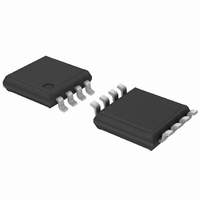
74LVC2G53DP,125 NXP Semiconductors, 74LVC2G53DP,125 Datasheet - Page 14

74LVC2G53DP,125
Manufacturer Part Number
74LVC2G53DP,125
Description
IC MUX/DEMUX 2X1 8TSSOP
Manufacturer
NXP Semiconductors
Series
74LVCr
Type
Analog Multiplexerr
Datasheet
1.74LVC2G53DC125.pdf
(28 pages)
Specifications of 74LVC2G53DP,125
Package / Case
8-TSSOP
Function
Multiplexer/Demultiplexer
Circuit
1 x 2:1
On-state Resistance
6 Ohm
Voltage Supply Source
Single Supply
Voltage - Supply, Single/dual (±)
1.65 V ~ 5.5 V
Current - Supply
0.1µA
Operating Temperature
-40°C ~ 125°C
Mounting Type
Surface Mount
Number Of Channels
1 Channel
On Resistance (max)
34 Ohm (Typ) @ 1.95 V
On Time (max)
6.7 ns (Typ) @ 1.95 V
Off Time (max)
6.8 ns (Typ) @ 1.95 V
Supply Voltage (max)
5.5 V
Supply Voltage (min)
1.65 V
Maximum Power Dissipation
250 mW
Maximum Operating Temperature
+ 125 C
Minimum Operating Temperature
- 40 C
Mounting Style
SMD/SMT
Number Of Switches
Single
Switch Current (typ)
0.0001 mA @ 5.5 V
Package
8TSSOP
Maximum On Resistance
195@1.95V Ohm
Maximum Propagation Delay Bus To Bus
2.5@1.95V@-40C to 125C|1.5@2.7V@-40C to 125C|1@3.6V@-40C to 125C|0.8@5.5V@-40C to 125C ns
Maximum Low Level Output Current
50 mA
Multiplexer Architecture
2:1
Maximum Turn-off Time
6.8(Typ)@1.95V ns
Maximum Turn-on Time
6.7(Typ)@1.95V ns
Power Supply Type
Single
Lead Free Status / RoHS Status
Lead free / RoHS Compliant
Lead Free Status / RoHS Status
Lead free / RoHS Compliant, Lead free / RoHS Compliant
Other names
74LVC2G53DP-G
74LVC2G53DP-G
935280383125
74LVC2G53DP-G
935280383125
NXP Semiconductors
Table 12.
At recommended operating conditions; voltages are referenced to GND (ground = 0 V); T
74LVC2G53
Product data sheet
Symbol
THD
f
α
Q
(−3dB)
Fig 19. Test circuit for measuring total harmonic distortion
iso
inj
Parameter
total harmonic distortion
−3 dB frequency response R
isolation (OFF-state)
charge injection
Additional dynamic characteristics
11.2 Additional dynamic characteristics
11.3 Test circuits
V
IL
or V
V
IH
IL
f i
600 Ω
0.1 μF
Conditions
f
C
R
see
C
f
i
i
= 600 Hz to 20 kHz; R
L
L
L
L
= 1 MHz; R
V
V
V
V
V
V
V
V
V
V
V
V
V
V
V
V
V
All information provided in this document is subject to legal disclaimers.
= 50 pF; V
= 50 Ω; C
= 50 Ω; C
= 0.1 nF; V
CC
CC
CC
CC
CC
CC
CC
CC
CC
CC
CC
CC
CC
CC
CC
CC
CC
Figure 21
S
Z
= 1.65 V
= 2.3 V
= 3.0 V
= 4.5 V
= 1.65 V
= 2.3 V
= 3.0 V
= 4.5 V
= 1.65 V
= 2.3 V
= 3.0 V
= 4.5 V
= 1.8 V
= 2.5 V
= 3.3 V
= 4.5 V
= 5.5 V
Rev. 6 — 27 September 2010
E
V
CC
L
L
L
I
gen
= 5 pF; see
= 5 pF; f
= 1 MΩ; see
= 0.5 V (p-p); see
GND
Y0
Y1
= 0 V; R
1
2
i
L
= 10 MHz;
switch
= 600 Ω;
gen
Figure 20
Figure 22
= 0 Ω;
0.5V
2-channel analog multiplexer/demultiplexer
Figure 19
CC
R L
C L
10 μF
D
switch
1
2
amb
Min
-
-
-
-
-
-
-
-
-
-
-
-
-
-
-
-
-
001aad394
= 25
V
V
S
IH
IL
74LVC2G53
0.078
0.078
0.078
Typ
0.260
200
300
300
300
−42
−42
−40
−40
3.3
4.1
5.0
6.4
7.5
°
C.
V
V
E
IL
IL
© NXP B.V. 2010. All rights reserved.
Max
-
-
-
-
-
-
-
-
-
-
-
-
-
-
-
-
-
Unit
%
%
%
%
MHz
MHz
MHz
MHz
dB
dB
dB
dB
pC
pC
pC
pC
pC
14 of 28


