74HC4053DB,118 NXP Semiconductors, 74HC4053DB,118 Datasheet - Page 4
74HC4053DB,118
Manufacturer Part Number
74HC4053DB,118
Description
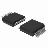
IC MUX/DEMUX TRIPLE 2X1 16SSOP
Manufacturer
NXP Semiconductors
Series
74HCr
Type
Analog Multiplexerr
Datasheet
1.74HC4053D653.pdf
(32 pages)
Specifications of 74HC4053DB,118
Package / Case
16-SSOP (0.200", 5.30mm Width)
Function
Multiplexer/Demultiplexer
Circuit
3 x 2:1
On-state Resistance
60 Ohm
Voltage Supply Source
Dual Supply
Voltage - Supply, Single/dual (±)
±2 V ~ 10 V
Current - Supply
16µA
Operating Temperature
-40°C ~ 125°C
Mounting Type
Surface Mount
Supply Voltage (max)
10 V
Supply Voltage (min)
2 V
Maximum Operating Temperature
+ 125 C
Minimum Operating Temperature
- 40 C
Mounting Style
SMD/SMT
Package
16SSOP
Maximum On Resistance
180@4.5V Ohm
Maximum Propagation Delay Bus To Bus
60@2V|12@4.5V|10@6V|8@±4.5V ns
Maximum Low Level Output Current
25 mA
Multiplexer Architecture
2:1
Maximum Turn-off Time
210@2V ns
Maximum Turn-on Time
220@2V ns
Power Supply Type
Single|Dual
Lead Free Status / RoHS Status
Lead free / RoHS Compliant
Lead Free Status / RoHS Status
Lead free / RoHS Compliant, Lead free / RoHS Compliant
Other names
74HC4053DB-T
74HC4053DB-T
935166800118
74HC4053DB-T
935166800118
Available stocks
Company
Part Number
Manufacturer
Quantity
Price
Company:

Part Number:
74HC4053DB,118
Manufacturer:
NXP Semiconductors
Quantity:
800


NXP Semiconductors
6. Pinning information
74HC_HCT4053
Product data sheet
Fig 4.
Fig 5.
Schematic diagram (one switch)
Pin configuration DIP16, SO16, and (T)SSOP16
GND
2Y1
2Y0
3Y1
3Y0
V
3Z
EE
from
logic
E
1
2
3
4
5
6
7
8
6.1 Pinning
74HCT4053
74HC4053
001aae127
All information provided in this document is subject to legal disclaimers.
16
15
14
13
12
11
10
9
V
2Z
1Z
1Y1
1Y0
S1
S2
S3
CC
Rev. 5 — 18 January 2011
Fig 6.
Triple 2-channel analog multiplexer/demultiplexer
(1) This is not a supply pin. The substrate is attached to this
74HC4053; 74HCT4053
V
EE
pad using conductive die attach material. There is no
electrical or mechanical requirement to solder this pad.
However, if it is soldered, the solder land should remain
floating or be connected to V
Pin configuration DHVQFN16
V
CC
index area
terminal 1
2Y0
3Y1
3Y0
V
3Z
EE
E
Transparent top view
2
3
4
5
6
7
74HCT4053
V
V
74HC4053
CC
CC
V
CC
(1)
CC
Y
Z
.
V
15
14
13
12
11
10
CC
001aad544
001aae128
© NXP B.V. 2011. All rights reserved.
2Z
1Z
1Y1
1Y0
S1
S2
V
V
EE
EE
4 of 32
Related parts for 74HC4053DB,118
Image
Part Number
Description
Manufacturer
Datasheet
Request
R

Part Number:
Description:
IC MUX/DEMUX TRIPLE 2X1 16SOIC
Manufacturer:
NXP Semiconductors
Datasheet:
Part Number:
Description:
IC MUX/DEMUX TRIPLE 2X1 16SOIC
Manufacturer:
NXP Semiconductors
Datasheet:

Part Number:
Description:
Analog Multiplexer Triple 2:1 16-Pin SO Bulk
Manufacturer:
NXP Semiconductors
Datasheet:
Part Number:
Description:
Encoders, Decoders, Multiplexers & Demultiplexers 2-ChanMux/Demux 10V
Manufacturer:
NXP Semiconductors
Datasheet:
Part Number:
Description:
Analog Multiplexer Triple 2:1 16-Pin SO T/R
Manufacturer:
NXP Semiconductors
Datasheet:
Part Number:
Description:
Encoders, Decoders, Multiplexers & Demultiplexers
Manufacturer:
NXP Semiconductors
Datasheet:
Part Number:
Description:
Manufacturer:
NXP Semiconductors
Datasheet:
Part Number:
Description:
NXP Semiconductors designed the LPC2420/2460 microcontroller around a 16-bit/32-bitARM7TDMI-S CPU core with real-time debug interfaces that include both JTAG andembedded trace
Manufacturer:
NXP Semiconductors
Datasheet:

Part Number:
Description:
NXP Semiconductors designed the LPC2458 microcontroller around a 16-bit/32-bitARM7TDMI-S CPU core with real-time debug interfaces that include both JTAG andembedded trace
Manufacturer:
NXP Semiconductors
Datasheet:
Part Number:
Description:
NXP Semiconductors designed the LPC2468 microcontroller around a 16-bit/32-bitARM7TDMI-S CPU core with real-time debug interfaces that include both JTAG andembedded trace
Manufacturer:
NXP Semiconductors
Datasheet:
Part Number:
Description:
NXP Semiconductors designed the LPC2470 microcontroller, powered by theARM7TDMI-S core, to be a highly integrated microcontroller for a wide range ofapplications that require advanced communications and high quality graphic displays
Manufacturer:
NXP Semiconductors
Datasheet:
Part Number:
Description:
NXP Semiconductors designed the LPC2478 microcontroller, powered by theARM7TDMI-S core, to be a highly integrated microcontroller for a wide range ofapplications that require advanced communications and high quality graphic displays
Manufacturer:
NXP Semiconductors
Datasheet:
Part Number:
Description:
The Philips Semiconductors XA (eXtended Architecture) family of 16-bit single-chip microcontrollers is powerful enough to easily handle the requirements of high performance embedded applications, yet inexpensive enough to compete in the market for hi
Manufacturer:
NXP Semiconductors
Datasheet:
Part Number:
Description:
The XA-S3 device is a member of Philips Semiconductors? XA(eXtended Architecture) family of high performance 16-bitsingle-chip microcontrollers
Manufacturer:
NXP Semiconductors
Datasheet: