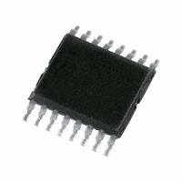
74LV4052PW,112 NXP Semiconductors, 74LV4052PW,112 Datasheet - Page 9

74LV4052PW,112
Manufacturer Part Number
74LV4052PW,112
Description
IC MUX/DEMUX DUAL 4X1 16TSSOP
Manufacturer
NXP Semiconductors
Series
74LVr
Type
Analog Multiplexerr
Datasheet
1.74LV4052DB118.pdf
(16 pages)
Specifications of 74LV4052PW,112
Function
Multiplexer/Demultiplexer
Circuit
2 x 4:1
On-state Resistance
60 Ohm
Voltage Supply Source
Single Supply
Voltage - Supply, Single/dual (±)
2.7 V ~ 3.6 V
Current - Supply
80µA
Operating Temperature
-40°C ~ 125°C
Mounting Type
Surface Mount
Package / Case
16-TSSOP (0.173", 4.40mm Width)
Multiplexer Configuration
Dual 4:1
Number Of Inputs
8
Number Of Outputs
2
Number Of Channels
2
Analog Switch On Resistance
250@1.2VOhm
Package Type
TSSOP
Power Supply Requirement
Single
Single Supply Voltage (min)
1V
Single Supply Voltage (typ)
3.3V
Single Supply Voltage (max)
6V
Dual Supply Voltage (min)
Not RequiredV
Dual Supply Voltage (typ)
Not RequiredV
Dual Supply Voltage (max)
Not RequiredV
Power Dissipation
400mW
Mounting
Surface Mount
Pin Count
16
Operating Temp Range
-40C to 125C
Operating Temperature Classification
Automotive
Lead Free Status / RoHS Status
Lead free / RoHS Compliant
Other names
74LV4052PW
74LV4052PW
935174950112
74LV4052PW
935174950112
Test conditions: V
Philips Semiconductors
NOTES TO FIGURES 6 AND 7:
1998 Jun 23
ADDITIONAL AC CHARACTERISTICS
Recommended conditions and typical values
GND = 0 V; t
GENERAL NOTES:
NOTES:
1. V
2. V
1. Adjust input voltage V
2. Adjust input voltage V
SYMBOL
Dual 4-channel analog multiplexer/demultiplexer
V
–100
f
Figure 6. Typical switch “OFF” signal feed-through as a
(dB)
V
(p–p)
max
C
–50
is
OS
is
S
0
is the input voltage at nY or nZ terminal, whichever is assigned as an input.
10
is the output voltage at nY or nZ terminal, whichever is assigned as an output.
0.1 mF
r
= t
Sine-wave distortion
f = 1 kHz
Sine-wave distortion
f = 10 kHz
Switch “OFF” signal feed through
Crosstalk between any two
switches/multiplexers
Crosstalk voltage between enable or
address input to any switch
(peak-to-peak value)
Minimum frequency response
(–3 dB)
Maximum switch capacitance
f
CC
10
2.5ns
R
= 3.0 V; GND = 0 V; V
2
L
function of frequency.
nY
is
is
PARAMETER
n
is 0 dBm level (0 dBm = 1 mW into 600 W).
is 0 dBm level at V
/nZ
10
3
Figure 8. Test circuit for measuring crosstalk between any two switches.
channel
ON
(a)
10
EE
V
(a) channel ON condition; (b) channel OFF condition.
4
CC
f (kHz)
= -3.0 V; R
2R
OS
L
2R
for 1 MHz (0 dBm = 1 mW into 50 W).
L
10
5
L
C
TYP.
0.80
0.40
2.40
1.20
nZ/nY
–50
–50
–60
–60
120
180
200
110
L
SV01635
= 50 W; R
5
n
10
UNIT
MHz
6
mV
dB
dB
GND
%
%
pf
SOURCE
9
V
3.0
6.0
3.0
6.0
3.0
6.0
3.0
6.0
3.0
6.0
3.0
6.0
(V)
CC
nY
= 1kW.
(dB)
n
/nZ
5
0
–5
10
V
Note 1
Note 1
Note 2
is(p–p)
2.75
5.50
2.75
5.50
(V)
2R
R
L
L
V
Figure 7. Typical frequency response.
CC
R
Figure 9 and 10
R
Figure 9 and 10
R
Figures 5 and 11
R
Figure 8
R
(S
and GND t
R
Figures 6, 8 and 9
10
L
L
L
L
L
L
n
2
channel
= 10 kW; C
= 10 kW; C
= 600 W; C
= 600 W; C
= 600 W; C
= 50 W; C
or E, square wave between V
OFF
r
10
V
= t
CC
L
3
(b)
L
L
L
L
L
f
= 50 pF
2R
= 6 ns) Figure 8
= 50 pf
= 50 pf
= 50 pf; f= 1 MHz
= 50 pf; f= 1 MHz
= 50 pf; f= 1 MHz
2R
L
CONDITIONS
L
10
4
f (kHz)
C
L
dB
Product specification
74LV4052
10
nZ/nY
CC
5
n
SV01663
SV01636
V
GND
os
10
6


