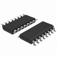
74LV4053D,118 NXP Semiconductors, 74LV4053D,118 Datasheet - Page 4

74LV4053D,118
Manufacturer Part Number
74LV4053D,118
Description
IC MUX/DEMUX TRIPLE 2X1 16SOIC
Manufacturer
NXP Semiconductors
Series
74LVr
Type
Analog Switchr
Datasheet
1.74LV4053BQ115.pdf
(26 pages)
Specifications of 74LV4053D,118
Package / Case
16-SOIC (0.154", 3.90mm Width)
Function
Multiplexer/Demultiplexer
Circuit
3 x 2:1
On-state Resistance
165 Ohm
Voltage Supply Source
Single Supply
Voltage - Supply, Single/dual (±)
2.7 V ~ 3.6 V
Current - Supply
80µA
Operating Temperature
-40°C ~ 125°C
Mounting Type
Surface Mount
Supply Voltage (max)
6 V
Supply Voltage (min)
1 V
Maximum Operating Temperature
+ 125 C
Minimum Operating Temperature
- 40 C
Mounting Style
SMD/SMT
Multiplexer Configuration
Triple 2:1
Number Of Inputs
6
Number Of Outputs
3
Number Of Channels
3
Analog Switch On Resistance
180@2VOhm
Package Type
SO
Power Supply Requirement
Single
Single Supply Voltage (min)
1V
Single Supply Voltage (typ)
3.3V
Single Supply Voltage (max)
6V
Dual Supply Voltage (min)
Not RequiredV
Dual Supply Voltage (typ)
Not RequiredV
Dual Supply Voltage (max)
Not RequiredV
Power Dissipation
500mW
Supply Current
0.08@6V@-40C to 125CmA
Mounting
Surface Mount
Pin Count
16
Operating Temp Range
-40C to 125C
Operating Temperature Classification
Automotive
Package
16SO
Maximum On Resistance
435@2V Ohm
Maximum Propagation Delay Bus To Bus
25(Typ)@1.2V|9(Typ)@2V|6(Typ)@2.7V|5(Typ)@3.3V|4(Typ)@4.5V|3(Typ)@6V ns
Maximum Low Level Output Current
25 mA
Multiplexer Architecture
2:1
Maximum Turn-off Time
95(Typ)@1.2V ns
Maximum Turn-on Time
125(Typ)@1.2V ns
Power Supply Type
Single
Lead Free Status / RoHS Status
Lead free / RoHS Compliant
Lead Free Status / RoHS Status
Lead free / RoHS Compliant, Lead free / RoHS Compliant
Other names
74LV4053D-T
74LV4053D-T
935175860118
74LV4053D-T
935175860118
NXP Semiconductors
5. Pinning information
Table 2.
74LV4053_4
Product data sheet
Symbol
E
V
GND
S1, S2, S3
1Y0, 2Y0, 3Y0
1Y1, 2Y1, 3Y1
1Z, 2Z, 3Z
V
Fig 5.
EE
CC
GND
2Y1
2Y0
3Y1
3Y0
V
3Z
EE
E
Pin configuration SOT38-4
and SOT109-1
Pin description
1
2
3
4
5
6
7
8
74LV4053
5.1 Pinning
5.2 Pin description
001aak424
Pin
6
7
8
11, 10, 9
12, 2, 5
13, 1, 3
14, 15, 4
16
16
15
14
13
12
11
10
9
V
2Z
1Z
1Y1
1Y0
S1
S2
S3
CC
Fig 6.
GND
2Y1
2Y0
3Y1
3Y0
V
3Z
EE
E
1
2
3
4
5
6
7
8
Rev. 04 — 10 August 2009
Description
enable input (active LOW)
supply voltage
ground supply voltage
select input
independent input or output
independent input or output
common output or input
supply voltage
Pin configuration
SOT338-1 and SOT403-1
74LV4053
001aak342
Triple single-pole double-throw analog switch
16
15
14
13
12
11
10
9
V
2Z
1Z
1Y1
1Y0
S1
S2
S3
CC
Fig 7.
index area
terminal 1
2Y0
3Y1
3Y0
V
3Z
EE
Pin configuration for
SOT763-1
E
Transparent top view
2
3
4
5
6
7
74LV4053
74LV4053
V
CC
© NXP B.V. 2009. All rights reserved.
(1)
15
14
13
12
11
10
001aak343
2Z
1Z
1Y1
1Y0
S1
S2
4 of 26


