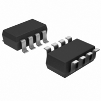
ADG3249BRJ-REEL Analog Devices Inc, ADG3249BRJ-REEL Datasheet - Page 10

ADG3249BRJ-REEL
Manufacturer Part Number
ADG3249BRJ-REEL
Description
IC MUX/DEMUX 2X1 SOT23-8
Manufacturer
Analog Devices Inc
Datasheet
1.ADG3249BRJ-R2.pdf
(12 pages)
Specifications of ADG3249BRJ-REEL
Rohs Status
RoHS non-compliant
Function
Multiplexer/Demultiplexer
Circuit
1 x 2:1
On-state Resistance
8 Ohm
Voltage Supply Source
Single Supply
Voltage - Supply, Single/dual (±)
2.3 V ~ 3.6 V
Current - Supply
0.01µA
Operating Temperature
-40°C ~ 85°C
Mounting Type
Surface Mount
Package / Case
SOT-23-8
Available stocks
Company
Part Number
Manufacturer
Quantity
Price
Part Number:
ADG3249BRJ-REEL7
Manufacturer:
ADI/亚德诺
Quantity:
20 000
ADG3249
Analog Switching
Bus switches can be used in many analog switching applications,
for example, video graphics. Bus switches can have lower on
resistance, smaller ON and OFF channel capacitance, and thus
improved frequency performance than their analog counterparts.
The bus switch channel itself, consisting solely of an NMOS
switch, limits the operating voltage (see TPC 1 for a typical
plot), but in many cases, this does not present an issue.
Multiplexing
Many systems, such as docking stations and memory banks,
have a large number of common bus signals. Common prob-
lems faced by designers of these systems include
•
•
Figure 11 shows an array of memory banks in which each ad-
dress and data signal is loaded by the sum of the individual
loads. If a bus switch is used as shown in Figure 12, the output
load on the memory address and data bits is halved. The speed
at which the selected bank’s data can flow is much improved
because the capacitance loading is halved and the switches
introduce negligible propagation delay. Bus noise is also reduced.
High Impedance during Power-Up/Power-Down
To ensure the high impedance state during power-up or power-
down, EN should be tied to V
minimum value of the resistor is determined by the current-
sinking capability of the driver.
Large delays caused by capacitive loading of the bus
Noise due to simultaneous switching of the address and data
bus signals
CC
through a pull-up resistor; the
–10–
Figure 11. All Memory Banks Are Permanently
Connected to the Bus
Figure 12. ADG3249 Used to Reduce Both Access
Time and Noise
ADDRESS
MEMORY
ADDRESS
MEMORY
MEMORY
MEMORY
MEMORY
MEMORY
BANK A
BANK B
BANK C
BANK D
MEMORY
MEMORY
MEMORY
MEMORY
BANK C
BANK A
BANK B
BANK D
DATA
DATA
REV. 0


