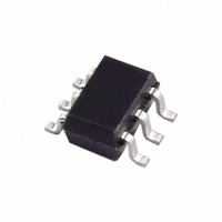
ADG849YKSZ-500RL7 Analog Devices Inc, ADG849YKSZ-500RL7 Datasheet - Page 3

ADG849YKSZ-500RL7
Manufacturer Part Number
ADG849YKSZ-500RL7
Description
IC SWITCH SPDT SC70-6
Manufacturer
Analog Devices Inc
Type
Analog Switchr
Datasheet
1.ADG849YKSZ-REEL.pdf
(12 pages)
Specifications of ADG849YKSZ-500RL7
Function
Switch
Circuit
1 x SPDT
On-state Resistance
600 mOhm
Voltage Supply Source
Single Supply
Voltage - Supply, Single/dual (±)
5V
Current - Supply
0.001µA
Operating Temperature
-40°C ~ 125°C
Mounting Type
Surface Mount
Package / Case
6-TSSOP, SC-88, SOT-363
Analog Switch Type
SPDT
No. Of Channels
1
Bandwidth
38MHz
On State Resistance Max
0.5ohm
Turn Off Time
9ns
Turn On Time
11ns
Supply Voltage Range
1.8V To 5.5V
Multiplexer Configuration
Single SPDT
Number Of Inputs
1
Number Of Outputs
2
Number Of Channels
1
Analog Switch On Resistance
1.1@3.6VOhm
Analog Switch Turn On Time
22ns
Analog Switch Turn Off Time
18ns
Package Type
SC-70
Power Supply Requirement
Single
Single Supply Voltage (min)
1.8V
Single Supply Voltage (typ)
3/5V
Single Supply Voltage (max)
5.5V
Dual Supply Voltage (min)
Not RequiredV
Dual Supply Voltage (typ)
Not RequiredV
Dual Supply Voltage (max)
Not RequiredV
Power Dissipation
0.00001W
Supply Current
0.001mA
Mounting
Surface Mount
Pin Count
6
Operating Temp Range
-40C to 125C
Operating Temperature Classification
Automotive
Lead Free Status / RoHS Status
Lead free / RoHS Compliant
Lead Free Status / RoHS Status
Lead free / RoHS Compliant, Lead free / RoHS Compliant
Other names
ADG849YKSZ500RLTR
Available stocks
Company
Part Number
Manufacturer
Quantity
Price
Company:
Part Number:
ADG849YKSZ-500RL7
Manufacturer:
Maxim
Quantity:
149
SPECIFICATIONS
Table 1. V
Parameter
ANALOG SWITCH
LEAKAGE CURRENTS
DIGITAL INPUTS
DYNAMIC CHARACTERISTICS
POWER REQUIREMENTS
1
2
The temperature range for the Y version is –40°C to +125°C.
Guaranteed by design, not subject to production test.
Analog Signal Range
On-Resistance (R
On-Resistance Match Between Channels
(∆R
On-Resistance Flatness (R
Source Off Leakage, I
Channel On Leakage, I
Input High Voltage, V
Input Low Voltage, V
Input Current
C
t
t
Break-Before-Make Time Delay, t
Charge Injection
Off Isolation
Channel-to-Channel Crosstalk
Bandwidth: –3 dB
Insertion Loss
THD + N
C
C
I
DD
ON
OFF
IN
S
D
, C
I
(Off )
, Digital Input Capacitance
INL
ON
S
)
or I
(On)
DD
INH
= 4.5 V to 5.5 V, GND = 0 V
ON
)
INL
S
INH
(Off )
D
, I
S
FLAT(ON)
(On)
2
)
BBM
1
±0.01
52
+25°C
0.5
0.6
0.05
0.095
0.13
0.18
±0.04
0.005
2.5
11
15
9
13
5
50
–64
–64
38
0.04
0.01
145
0.001
–40°C to
+85°C
0.7
0.11
0.22
17
14
Rev. 0| Page 3 of 12
–40°C to
+125°C
0 V to V
0.8
0.125
0.24
2.0
0.8
±0.1
18
15
1
1.0
DD
Unit
V
Ω typ
Ω max
Ω typ
Ω max
Ω typ
Ω max
nA typ
nA typ
V min
V max
µA typ
µA max
pF typ
ns typ
ns max
ns typ
ns max
ns typ
ns min
pC typ
dB typ
dB typ
MHz typ
dB typ
%
pF typ
pF typ
µA typ
µA max
Test Conditions/Comments
V
See Figure 15
V
V
V
V
see Figure 16
V
see Figure 17
V
R
V
R
V
R
see Figure 19
V
R
see Figure 21
R
see Figure 22
R
R
R
Vs = 2 V p-p
V
L
L
L
L
L
L
L
L
S
S
S
DD
S
S
IN
S
S
S
DD
= 50 Ω, C
= 50 Ω, C
= 50 Ω, C
= 50 Ω, C
= 50 Ω, C
= 50 Ω, C
= 50 Ω, C
= 32 Ω, f = 20 Hz to 20 kHz,
= 0 V to V
= 0.85 V, I
= 0 V to V
= 4.5 V/1 V, V
= V
= 3 V, see Figure 18
= 3 V, see Figure 18
= 0 V, R
= V
= 5.5 V
= 5.5 V, Digital Inputs = 0 V or 5.5 V
D
INL
= 1 V, or V
or V
S
= 0 Ω, C
L
L
L
L
L
L
L
DD
DD
DS
INH
= 35 pF
= 35 pF
= 35 pF, V
= 5 pF, f = 100 kHz
= 5 pF, f = 100 kHz,
= 5 pF, see Figure 23
= 5 pF, see Figure 23
, I
, I
= –100 mA
D
DS
DS
= 1 V/4.5 V,
S
= –100 mA
= –100 mA
= V
L
= 1 nF, see Figure 20
D
S1
= 4.5 V,
= V
S2
ADG849
= 3 V,


