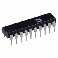
ADG333ABNZ Analog Devices Inc, ADG333ABNZ Datasheet - Page 10

ADG333ABNZ
Manufacturer Part Number
ADG333ABNZ
Description
IC SWITCH QUAD SPDT 20DIP
Manufacturer
Analog Devices Inc
Type
Analog Switchr
Datasheet
1.ADG333ABRZ.pdf
(12 pages)
Specifications of ADG333ABNZ
Function
Switch
Circuit
4 x SPDT
On-state Resistance
45 Ohm
Voltage Supply Source
Single Supply
Voltage - Supply, Single/dual (±)
12V
Current - Supply
0.01µA
Operating Temperature
-40°C ~ 85°C
Mounting Type
Through Hole
Package / Case
20-DIP (0.300", 7.62mm)
Analog Switch Type
SPDT
No. Of Channels
4
On State Resistance Max
45ohm
Turn Off Time
80ns
Turn On Time
90ns
Supply Voltage Range
3V To 30V
Operating Temperature Range
-40°C To +85°C
Multiplexer Configuration
Quad SPDT
Number Of Inputs
4
Number Of Outputs
8
Number Of Channels
4
Analog Switch On Resistance
45@±15VOhm
Analog Switch Turn On Time
110ns
Analog Switch Turn Off Time
100ns
Package Type
PDIP N
Power Supply Requirement
Single/Dual
Single Supply Voltage (min)
3V
Single Supply Voltage (typ)
12V
Single Supply Voltage (max)
30V
Dual Supply Voltage (min)
±3V
Dual Supply Voltage (typ)
±5/±9/±12/±15V
Dual Supply Voltage (max)
±20V
Power Dissipation
3.77mW
Supply Current
0.25@±15VmA
Mounting
Through Hole
Pin Count
20
Operating Temp Range
-40C to 85C
Operating Temperature Classification
Industrial
Package
20PDIP N
Maximum On Resistance
45@±15V Ohm
Maximum High Level Output Current
20 mA
Maximum Turn-off Time
100(Typ)@12V ns
Maximum Turn-on Time
110(Typ)@12V ns
Switch Architecture
SPDT
Power Supply Type
Single|Dual
Lead Free Status / RoHS Status
Lead free / RoHS Compliant
Lead Free Status / RoHS Status
Lead free / RoHS Compliant, Lead free / RoHS Compliant
Available stocks
Company
Part Number
Manufacturer
Quantity
Price
Part Number:
ADG333ABNZ
Manufacturer:
ADI/亚德诺
Quantity:
20 000
ADG333A
TEST CIRCUITS
V
S
R
ON
Figure 14. On Resistance
= V
V
V
S
D
1
V
+10V
S
–10V
/I
S
V
DS
1
V
D
R
IN
D
I
DS
IN
IN
Figure 20. Off Isolation
0.1µF
IN
0.1µF
GND
SB
SA
0.1µF
GND
SB
SA
GND
GND
0.1µF
V
V
0.1µF
DD
DD
V
V
S
V
D
DD
DD
0.1µF
D
V
V
V
V
DD
DD
D
DD
DD
V
V
D
SA
SS
SS
D
V
V
SS
SS
V
V
V
V
SS
SS
SS
SS
R
300Ω
L
R
300Ω
L
C
10nF
V
L
S
Figure 18. Break-Before-Make Delay, t
R
75Ω
L
C
35pF
I
S
L
C
35pF
V
L
(OFF)
V
A
OUT
V
OUT
OUT
V
Figure 19. Charge Injection
Figure 17. Switching Times
OUT
Figure 15. Off Leakage
Rev. A | Page 10 of 12
S
D
+10V
–10V
+3V
0V
0V
V
V
V
IN
S
S
3V
0V
V
3V
0V
0V
S
V
OUT
V
V
IN
OUT
V
V
V
OPEN
OUT
IN
D
75Ω
V
R
IN1
Figure 21. Channel-to-Channel Crosstalk
50%
t
L
ON
50%
50%
t
0.1µF
OFF
t
OPEN
NC
GND
Q
S
INJ
0.1µF
V
V
= C
D
50%
DD
DD
S
50%
L
NC = NO CONNECT
×
V
V
D
Figure 16. On Leakage
50%
SS
∆V
SS
OUT
S
CHANNEL-TO-CHANNEL
CROSSTALK
20
×
D
LOG |V
75Ω
∆V
V
NC
IN2
OUT
S
/V
I
D
OUT
(ON)
A
|
V
D


