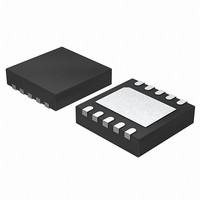
ISL54209IRTZ Intersil, ISL54209IRTZ Datasheet - Page 11

ISL54209IRTZ
Manufacturer Part Number
ISL54209IRTZ
Description
IC USB SWITCH DUAL SPDT 10TDFN
Manufacturer
Intersil
Datasheet
1.ISL54209IRTZ.pdf
(19 pages)
Specifications of ISL54209IRTZ
Function
USB Switch
Circuit
2 x SPDT
On-state Resistance
20 Ohm
Voltage Supply Source
Single Supply
Voltage - Supply, Single/dual (±)
2.5 V ~ 5 V
Current - Supply
7µA
Operating Temperature
-40°C ~ 85°C
Mounting Type
Surface Mount
Package / Case
10-TDFN Exposed Pad
Lead Free Status / RoHS Status
Lead free / RoHS Compliant
Detailed Description
The ISL54209 device is a dual single pole/double throw
(SPDT) analog switch that operates from a single DC
power supply in the range of 2.5V to 5.0V. It was
designed to function as a dual 2 to 1 multiplexer to select
between USB differential data signals and audio L and R
stereo signals. It comes in tiny µTQFN and TDFN
packages for use in MP3 players, PDAs, cellular phones
and other personal media players.
The part consists of two 2.5Ω audio switches and two 5Ω
USB switches. The audio switches can accept signals that
swing below ground. They were designed to pass audio
left and right stereo signals, that are ground referenced,
with minimal distortion. The USB switches were designed
to pass high-speed USB differential data signals with
minimal edge and phase distortion.
The ISL54209 was specifically designed for MP3 players,
personal media players and cellular phone applications
that need to combine the audio headphone jack and the
USB data connector into a single shared connector,
thereby saving space and component cost. “Typical
Application Block Diagrams” on page 10 of this
functionality are shown in Figures 8 and 9.
The ISL54209 has a single logic control pin (IN) that
selects between the audio switches and the USB
switches. This pin can be driven Low or High to switch
between the audio CODEC drivers and USB transceiver of
the MP3 player or cellular phone. The ISL54209 also
contains a logic control pin (CTRL) that when driven Low
while IN is Low, opens all switches and puts the part into
a low power state, drawing typically 1nA of I
Detailed descriptions of the two types of switches are
provided in the following sections.
Audio Switches
The two audio switches (L, R) are 2.5Ω switches that can
pass signals that swing below ground by as much as
1.5V. They were designed to pass ground reference
stereo signals with minimal insertion loss and very low
distortion over a ±1V signal range.
Crosstalk between the audio channels is -110dB over the
audio band. Crosstalk between the audio channel and
USB channel is -95dB at 100kHz. These switches have
excellent OFF-isolation, 114dB, over the audio band with
a 32Ω load.
Over a signal range of ±1V (0.707V
VDD > 2.7V, these switches have an extremely low r
resistance variation. They can pass ground referenced
audio signals with very low distortion (<0.06% THD+N)
when delivering 15.6mW into a 32Ω headphone speaker
load. See Figures 10 and 11.
These switches are bi-directional switches. In typical
applications, the audio drivers would be connected at the
L and R side of the switch and the speaker loads would
be connected at the COM side of the switch.
11
RMS
) with
DD
current.
ISL54209
ON
The audio switches are active (turned ON) whenever the
IN voltage is ≤ 0.5V or floating and the CTRL voltage ≥ to
1.4V.
USB Switches
The two USB switches (D+, D-) are bidirectional switches
that can pass rail-to-rail signals. When powered with a
3.3V supply, these switches have a nominal r
over the signal range of 0V to 400mV with a r
of 0.45Ω. The r
switches over this signal range is only 0.05Ω ensuring
minimal impact by the switches to USB high speed signal
transitions. As the signal level increases, the r
resistance increases. At a signal level of 3.3V, the switch
resistance is nominally 25Ω.
The USB switches were specifically designed to pass USB
2.0 high-speed (480Mbps) differential signals typically in
the range of 0V to 400mV. They have low capacitance
and high bandwidth to pass the USB high-speed signals
with minimum edge and phase distortion to meet USB
2.0 high speed signal quality specifications. See
Figure 12.
The USB switches can also pass USB full-speed signals
(12Mbps) with minimal distortion and meet all the USB
requirements for USB 2.0 full-speed signaling. See
Figure 13 for Full-speed Eye Pattern taken with switch in
the signal path.
The USB switches are active (turned ON) whenever the
IN voltage is ≥ to 1.4V.
COM+, COM-, 1D-, 1D+, 2D-, AND 2D+ ARE
OVERVOLTAGE TOLERANT UP TO 5.5V AND
DOWN TO -1.5V
For normal operation, the signal range for the USB
switches is from -1V to V
the signal voltage at D- and D+ should not be allowed
to exceed the V
more than -1.0V. However, the ISL54209, with a VDD
supply voltage in the range of 0V to 5.0V, can
withstand an overvoltage of up to 5.5V or down to
-1.5V applied at its COM pins (COM-, COM+) and/or
USB signal pins (1D-, 1D+, 2D-, 2D+) without
damage. In this overvoltage condition, the part draws
<1mA of current and causes no stress to the IC.
Note: When in the overvoltage state, the fault voltage
at a COM pin will pass thru the USB switch to the signal
side of the switch, so the media player’s USB
transceiver must have protection circuitry to protect it
from damage.
ISL54209 Operation
The following will discuss using the ISL54209 in the
“Typical Application Block Diagrams” on page 10 shown
in Figures 8 and 9.
VDD SUPPLY
The DC power supply connected at VDD pin provides the
required bias voltage for proper switch operation. The
ON
DD
matching between the D+ and D-
voltage rail or go below ground by
DD
. During normal operation,
ON
ON
ON
June 10, 2010
of 5Ω
flatness
FN6627.4


