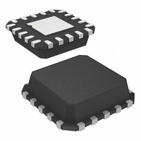
ISL54405IRTZ-T Intersil, ISL54405IRTZ-T Datasheet - Page 9

ISL54405IRTZ-T
Manufacturer Part Number
ISL54405IRTZ-T
Description
IC MUX STEREO 2:1 CD/MP3 16-TQFN
Manufacturer
Intersil
Datasheet
1.ISL54405IRUZ-T.pdf
(19 pages)
Specifications of ISL54405IRTZ-T
Function
Switch
Circuit
2 x SPDT
Voltage Supply Source
Single Supply
Voltage - Supply, Single/dual (±)
3 V ~ 3.6 V
Operating Temperature
-40°C ~ 85°C
Mounting Type
Surface Mount
Package / Case
16-WFQFN Exposed Pad
Lead Free Status / RoHS Status
Lead free / RoHS Compliant
Available stocks
Company
Part Number
Manufacturer
Quantity
Price
Company:
Part Number:
ISL54405IRTZ-T
Manufacturer:
JENNIC
Quantity:
1 200
SPDT Switch Cell Architecture and Performance
Characteristics
The normally open (L
the SPDT switches are T-Type switches that have a typical
r
resistance (1.9Ω) and r
insertion loss and minimal distortion to applications that
require hi-fidelity signal reproduction.
The SPDT switch cells have internal charge pumps that
allow for signals to swing below ground. They were
specifically designed to pass audio signals that are ground
referenced and have a swing of ± 2.828V
either 10k/20kΩ (receiver) or 32Ω (headphone) loads.
Each switch cell incorporates special circuitry to gradually
decrease the switch resistance when transitioning from the
OFF-state (high impedance) to the ON state (1.9Ω). The
gradual decrease in the switch resistance provides for a slow
ramp of the voltage at the load side of the switch which helps
to eliminate click and pops in the speaker by suppressing the
transient during switching events. The output voltage ramp
time is determined by the capacitor value of the soft-start
capacitor connected at the CAP_SS pin. With a 0.1µF
ceramic chip capacitor the ramp time is approximately
4.6V/s. The slow ramping of the signal at the output can be
disabled by floating the CAP_SS pin.
In addition to the slow ramp feature (soft-start feature) of the
in line switches, the part has special click and pop (C/P)
shunt circuitry at each of the signal pins (L, R, L
and R
activated depending on the logic levels applied at the AC/DC
and DIR_SEL control pins. This shunt circuitry serves two
functions:
If the AC/DC pin is driven LOW, all C/P shunt circuitry at all
the signal pins (L, R, L1, R1, L2, and R2) are deactivated
and not operable.
If the AC/DC pin is driven HIGH then the logic at the
DIR_SEL pin will determine whether the L and R (COM) C/P
shunt circuitry is activated or the L1, L2, R1, and R2 (NOx,
NCx) C/P shunt circuitry is activated. When the DIR_SEL is
driven LOW, the L1, R1, L2, R2 C/P shunt circuitry will be
activated while the L and R C/P shunt circuitry will be
deactivated. When the DIR_SEL is driven HIGH the L and R
C/P shunt circuitry will be activated while the L1, R1, L2, R2
C/P shunt circuitry will be deactivated. Note: Shunt circuitry
that is activated will be turned ON when a switch cell is
turned OFF and will be OFF when a switch cell is turned ON.
ON
1. In an AC coupled application they are activated and
2. For superior muting the C/P shunt circuitry is activated
directed to the source side of the switch to suppress or
eliminate click/pop noise in the speaker load when
powering up or down of the audio CODEC drivers.
and directed to the load side of the switch which gives
>120dB of off-isolation when driving a 10k/20kΩ receiver
load with an audio signal in the range of 20Hz to 22kHz.
of 1.9Ω and an off-isolation of >120dB. The low on-
2
). A pin’s C/P shunt circuitry is activated or de-
2
, R
ON
2
) and normally closed (L
flatness (0.003Ω) provide very low
9
PEAK
while driving
1
, L
1
2
, R
, R
1
1
) of
,
ISL54405
Supply Voltage, Signal Amplitude, Grounding
The power supply connected at VDD or the 5V_SUPPLY pin
provides power to the ISL54405 part. The ISL54405 is a
single supply device that was designed to be operated with a
3.3V ±10% DC supply connected at the VDD pin or a 5V
±10% DC supply connected at the 5V_SUPPLY pin.
It was specifically designed to accept ground referenced
2V
driving either 10k/20kΩ receiver loads or 32Ω headphone
loads.
When using the part in a 3.3V application the 5V_Supply pin
should be left floating. A 0.1µF decoupling capacitor should
be connected from the VDD pin to ground to minimize power
supply noise and transients. This capacitor should be
located as close to the pin as possible.
The part also has a 5V supply pin (5V_Supply) to allow it to
be used in 5V ±10% applications. Special circuitry within the
device converts the 5V, connected at the 5V_Supply pin, too
3.3V to properly power the internal circuitry of the device.
When using the part in a 5V application the VDD pin should
be left floating. A 0.1µF decoupling capacitor should be
connected from the 5V_Supply pin to ground to minimize
power supply noise. This capacitor should be located as
close to the pin as possible.
Grounding of the ISL54405 should follow a star configuration
(see Figure 7). All grounds of the IC should be directly
connected to the power supply ground return without
cascading to other grounds. This configuration isolates
shunt currents of the Click and Pop transients from the IC
ground and optimizes device performance.
DIR_SEL
Mute Operation
When the MUTE logic pin is driven HIGH the part will go into
the Mute State. In the Mute State all switches of the SPDTs
are OPEN while the T-Shunt switches are closed. In addition
any activated click and pop shunt circuitry at the signal pins
is turned ON.
See “Logic Control” on page 10 for more details.
AC/DC
MUTE
RMS
SEL
FIGURE 7. STAR GROUNDING CONFIGURATION
R
L
(± 2.828V
ISL54405
+3.3V
CONTROL
LOGIC
VDD
PEAK
GND1
) audio signals at its signal pins while
GND2
GND3
L1
L2
R1
R2
0.1µF
June 5, 2008
FN6699.1


