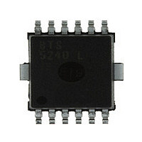
BTS5240LXT Infineon Technologies, BTS5240LXT Datasheet - Page 11

BTS5240LXT
Manufacturer Part Number
BTS5240LXT
Description
Manufacturer
Infineon Technologies
Datasheet
1.BTS5240LXT.pdf
(17 pages)
Specifications of BTS5240LXT
Switch Type
High Side
Power Switch Family
BTS 5240
Input Voltage
-10 to 16V
Power Switch On Resistance
11mOhm
Output Current
4.1A
Number Of Outputs
Dual
Mounting
Surface Mount
Supply Current
1.6mA
Package Type
DSO
Operating Temperature (min)
-40C
Operating Temperature (max)
150C
Operating Temperature Classification
Automotive
Pin Count
12
Power Dissipation
1.4W
Lead Free Status / Rohs Status
Not Compliant
Input circuit ( ESD protection ), IN1 or IN2
The use of ESD zener diodes as voltage clamp
at DC conditions is not recommended.
Sense-Status output, IS1 or IS2
ON-State: Normal operation: I S = I L / kILIS
V IS = I S * R IS ;
ESD zener diode: V
ON-State: Fault condition so as thermal shut down
or current limitation
V fault = 6 V typ ; V
OFF-State diagnostic condition:
Open Load, if V
ESD-Zener diode: 6,1V typ., max. 5mA; R
at 1,6mA.. The use of ESD zener diodes as voltage clamp
at DC conditions is not recommended.
IN
V
V
ESD-ZD
V
fault
f
f
Int. 5V
R
I
ESD-ZD
IS
ESD-ZD
I
GND
I
GND
Sense output
logic
Sense output
logic
OUT
GND
GND
R IS = 1k nominal
fault
R IS > 500
ESD
> 3 V typ.; IN low
I
I
ESD-
ZD
< V
IS
IS - ST
= 6,1 V typ., max. 14 mA ;
R
R
ESD
V
IS
IS
fault
V
IS
R
under all conditions
IS
ST(ON)
< 375
Page 11
Inductive and overvoltage output clamp,
OUT1 or OUT2
V Out clamped to V Out(CL) = -15 V typ.
Overvolt. Protection of logic part
OUT1 or OUT2
V Z1 = 6,1V typ., V Z2 = 47V typ., R GND = 150 ,
R IS = 1k , R I = 3,5k typ.
V
V
Z
Z
R
IS
IN
IS
GND
GND
R
I
V
Z1
Logic
R
Power GND
Power GND
G N D
PR O F ET
V
+V bb
+V bb
G N D
Z2
OUT
OUT
Sig na l G N D
V
V
OUT
OUT
+ V bb
BTS 5240L
2005-06-03


