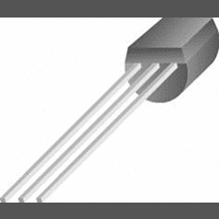
J111-E3 Vishay, J111-E3 Datasheet - Page 2

J111-E3
Manufacturer Part Number
J111-E3
Description
51K2069
Manufacturer
Vishay
Datasheet
1.J111-E3.pdf
(6 pages)
Specifications of J111-E3
Breakdown Voltage Vbr
-55V
Zero Gate Voltage Drain Current Idss
20mA
Gate-source Cutoff Voltage Vgs(off) Max
-10V
Power Dissipation Pd
360mW
Operating Temperature Range
-55°C To +150°C
No. Of Pins
3
Rohs Compliant
Yes
The graph in Figure 3 is useful in estimating r
at any given value of V
to its specific value at V
r
trol of r
AN105
DS
–2.5 V
V
2
GS
is shown as greater than 100:1, although for best con-
–1.5 V
= –3.0 V
1000
–400
100
10
DS
1
0 V
0
D
G
S
a range of 10:1 is normally used.
–200
I
D
Figure 3. Normalized r
V
0 V
DS
r
200
0.2
DS
0.1 V
1 – V
–1.5 V
GS
GS
–200
V
200
0.4
V
. The resistance is normalized
GS
r
V
= 0 V. The dynamic range of
GS
GS
DS(on)
DS
= –3.0 V
/V
–2.5 V
V
(mV)
3
2
1
GS(off)
GS(off)
400
0.6
DS
V
Data
5
GS
V
–1.5 V
–2.5 V
DS
= 0 V
0.8
10
(V)
DS
values
–3.0 V
1.0
Siliconix offers a family of n-channel FETs specifically
intended for use as voltage-controlled resistors. These de-
vices have r
where VCR2N = 20 – 60
VCR7N = 4 k – 8 k .
Applications for VCRs
A simple application of a FET VCR is shown in Figure 4,
the circuit for a voltage divider attenuator.
It is assumed that the output voltage is not so large as to
push the VCR out of the linear resistance region, and that
the r
Signal Distortion: Causes
Figure 2 shows that the bias lines bend down as V
increases in a positive direction toward the pinch-off voltage
of the FET. The bending of the bias lines results in a change
in r
note that the distortion occurs in both the first and third
quadrants. Distortion results because the channel depletion
layer increases as V
pinch-off condition is reached when V
Figure 5 shows how the current has an opposite effect in the
third quadrant, increasing negatively with an increasingly
negative V
gate-to-channel junction when the drain signal exceeds the
negative gate bias voltage.
V
V
DS
OUT
OUT(min)
V
DS
, and hence the distortion encountered in VCR circuits;
IN
is not shunted by the load.
DS
R
Figure 4. Simple Attenuator Circuit
V
DS(on)
. This is due to the forward conduction of the
IN
R
r
V
r
DS
DS
IN
values ranging from 20
R
DS
r
DS(on)
r
+
–
DS(on
reduces the drain current so that a
V
GS
)
, VCR4N = 200 – 600
DS
VCR
= V
GS
10-Mar-97
to 4,000 ,
– V
Siliconix
V
GS(off)
OUT
(1)
(2)
DS
,
.


