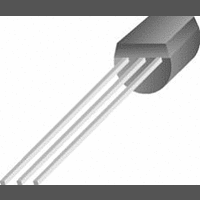
J111-E3 Vishay, J111-E3 Datasheet - Page 3

J111-E3
Manufacturer Part Number
J111-E3
Description
51K2069
Manufacturer
Vishay
Datasheet
1.J111-E3.pdf
(6 pages)
Specifications of J111-E3
Breakdown Voltage Vbr
-55V
Zero Gate Voltage Drain Current Idss
20mA
Gate-source Cutoff Voltage Vgs(off) Max
-10V
Power Dissipation Pd
360mW
Operating Temperature Range
-55°C To +150°C
No. Of Pins
3
Rohs Compliant
Yes
Siliconix
10-Mar-97
V
V
V
IN
IN
IN
R
Figure 5. Simple Attenuator Circuit
1
R
R
2
3
+
–
R
V
R
R
R
GG
1
2
V
G
+
3
–
= R
CONTROL
R
+
VCR Linearization
2
Figure 6.
Anode
V
Diode
Figure 7.
3
GS
// 10(r
+V
–V
DS
0
//R
load
VCR
VCR
//R
VCR
Diode
Cathode
when Signal
Swings Negative
1
)
V
V
V
OUT
OUT
OUT
Reducing Signal Distortion
The majority of VCR applications require that signal
distortion be kept to a minimum. Also, numerous
applications require large signal handling capability. A
simple feedback technique may be used to reduce
distortion while permitting large signal handling
capability; a small amount of drain signal is coupled to the
gate through a resistor divider network, as shown in
Figure 6.
The application of a part of the positive drain signal to the
gate causes the channel depletion layer to decrease, with
a corresponding increase in drain current. Increasing the
drain current for a given drain voltage tends to linearize
the V
negative voltage is coupled to the gate to reduce the
amount of drain-gate forward bias. This in turn reduces
the drain current and linearizes the bias lines. Now the
channel resistance is dependent on the dc gate control
voltage and not on the drain signal, unless the V
– V
Figure 6 couple the drain signal to the gate; the resistor
values are equal, so that symmetrical voltage-current
characteristics are produced in both quadrants. The
resistors must be sufficiently large to provide minimum
loading to the circuit:
Typically, 470-k
plications. R
[(r
The feedback technique used in Figure 6 requires that the
gate control voltage, V
ure 5 for the same r
tween the resistor junction and the FET gate will over-
come this problem. The circuit is shown in Figure 7 and
allows the gate control voltage to be the same value as that
voltage used without a feedback circuit, while preserving
the advantages to be gained through the feedback tech-
nique.
R
V
2
DS(on)
O
= R
GS(off)
GS
3
V
bias curves. On the negative half-cycle, a small
I
R
(r
locus is approached. Resistors R
10 [R
L
DS(on)
1
) + R
is selected so that the ratio of r
r
DS(on)
1
1
r
] give the desired output voltage, or:
DS
resistors will work well for most ap-
DS
R
L
(max) R
GG
)
value. Use of a floating supply be-
R
L
, be twice as large as V
R
1
L
]
AN105
DS(on)
2
and R
GS
DS
in Fig-
= V
R
(3)
(4)
3
L
GS
3
in
to


