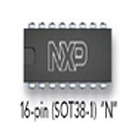
TDA8444 NXP Semiconductors, TDA8444 Datasheet - Page 6

TDA8444
Manufacturer Part Number
TDA8444
Description
Manufacturer
NXP Semiconductors
Datasheet
1.TDA8444.pdf
(16 pages)
Specifications of TDA8444
Number Of Channels
8
Resolution
6b
Interface Type
Serial (I2C)
Single Supply Voltage (typ)
12V
Dual Supply Voltage (typ)
Not RequiredV
Architecture
Current Steering
Power Supply Requirement
Single
Output Type
Voltage
Integral Nonlinearity Error
±0.5LSB
Single Supply Voltage (min)
4.5V
Single Supply Voltage (max)
13.2V
Dual Supply Voltage (min)
Not RequiredV
Dual Supply Voltage (max)
Not RequiredV
Operating Temp Range
-20C to 70C
Operating Temperature Classification
Commercial
Mounting
Through Hole
Pin Count
16
Package Type
PDIP
Lead Free Status / Rohs Status
Compliant
Available stocks
Company
Part Number
Manufacturer
Quantity
Price
Part Number:
TDA8444
Manufacturer:
PHILIPS/飞利浦
Quantity:
20 000
Company:
Part Number:
TDA8444/N2
Manufacturer:
Philips
Quantity:
1 189
Part Number:
TDA8444/N2
Manufacturer:
PHILIPS/飞利浦
Quantity:
20 000
Part Number:
TDA8444AT
Manufacturer:
NXP/恩智浦
Quantity:
20 000
Part Number:
TDA8444P
Manufacturer:
PHILIPS/飞利浦
Quantity:
20 000
Company:
Part Number:
TDA8444P/N4
Manufacturer:
PHI
Quantity:
8 000
Part Number:
TDA8444P/N4
Manufacturer:
PHILIPS/飞利浦
Quantity:
20 000
Philips Semiconductors
The circuit will not react to other combinations of the
4 instruction bits I3 to I0 than 0 or F, but will still generate
an acknowledge. The difference between
instruction 0 and F is only important when more than one
data byte is sent within one transmission. Instruction 0
causes the data bytes to be written into the DAC-latches
with consecutive subaddresses starting with the
subaddress given in the instruction byte (auto-increment of
subaddress), while instruction F will cause a consecutive
writing of the data bytes into the same DAC-latch whose
subaddress was given in the instruction byte. In case of
only one data byte the DAC-latch with the subaddress
equal to the subaddress in the instruction byte will receive
the data.
Valid subaddresses are: 0H to 7H.
The subaddresses correspond to DAC0 to DAC7.
The Auto-Increment (AI) function of instruction 0,
however, works on all possible subaddresses 0 to F in
such a way that next to subaddress F, subaddress 0 will
follow, and so on.
The data will be latched into the DAC-latch on the
positive-going edge of the acknowledge related clock
pulse.
The specification of the SCL and SDA I/O meets the
I
voltage pulses on pins 3 and 4, zener diodes are
LIMITING VALUES
In accordance with the Absolute Maximum Rating System (IEC 134).
QUALITY SPECIFICATION
In accordance with “SNW-FQ-611-E” .
1999 Apr 29
2
V
I
P
V
I
T
T
CC
n
C-bus specification. For protection against positive
stg
amb
CC
(max)
i(n)
Octuple 6-bit DACs with I
SYMBOL
supply voltage
supply current
maximum power dissipation
input voltage
current in all pins except V
storage temperature
operating ambient temperature
pins SDA and SCL
pins V
MAX
, A0 to A2 and DAC0 to DAC7
PARAMETER
2
C-bus
CC
and V
EE
6
connected between these pins and V
normal bus line voltage should not exceed 5.5 V.
The address inputs A0, A1 and A2 can be easily
programmed by either a connection to V
(An = 1). If the inputs are left floating the result will be
An = 1.
V
The V
output voltage swing. The maximum DAC output voltage
will be equal to V
is maintained. This enables a higher voltage resolution for
smaller output swings.
DACs
The DACs consist of a 6-bit data-latch, current switches
and an opamp. The current sources connected to the
switches have values with weights 2
switched on currents is converted by the opamp into a
voltage between approximately 0.5 and 10.5 V if
V
protected against V
DAC outputs should not exceed 2 nF in order to prevent
possible oscillations at certain levels. The temperature
coefficient for each of the outputs remains in all possible
conditions well below 0.1 LSB per Kelvin.
MAX
MAX
= V
MAX
CC
input gives a means of compressing the DAC
= 12 V. The DAC outputs are short-circuit
0.5
10
0.5
0.5
0.5
65
20
MAX
MIN.
CC
+ V
TDA8444; TDA8444T;
and V
DAC(min)
+18
+40
500
+5.9
+5.9
V
+150
+70
EE
10
CC
. Capacitive load on the
, while the 6-bit resolution
MAX.
+ 0.5
0
Product specification
TDA8444AT
to 2
EE
. This means that
EE
5
. The sum of the
(An = 0) or V
V
mA
mW
V
V
V
mA
C
C
UNIT
CC


